

DARPA Connected Micro Impants: Criminal and Scientific Misconduct
![]()

![]()
![]()
![]() Criminal and
Scientific Misconduct Involving Neural Prosthesis Research
Criminal and
Scientific Misconduct Involving Neural Prosthesis Research
Question: Why are remote radio towers and signalling grids being developed to access the micro-implants described? This goes beyond mind control. It wanders into the realm of physical control. Very very dangerous!
Note: This is not a new leak. It has been on the server since 2002 but for some reason someone has been accessing it quite actively recently.
Report by David A Larson_First Edit in .pdf
Criminal and Scientific Misconduct Involving Neural Prosthesis Research Funded by the
NIH/NINDS/NPP and The Alfred E. Mann Foundation
David A. Larson
lars1212@verizon.net
Articles of Evidence:
The photos contained in this document are of microstimulator devices that were surgically recovered and
analyzed by using microscopy and by materials charcterization techniques. The recovered devices are an
exact match for the devices that were developed by research scientists Joseph Schulman, Gerald Loeb and
Philip Troyk under contract from the National Institutes of Health. There are about 4 contracts involved, but
the initial contract was #N01-NS5-2325 and funded by the NIH/NINDS/NPP. More information regarding
these contracts can be found at the NIH Neural Prosthesis Project website. The following list briefly outlines
some of the evidence presented in this document:
1. Microstimulator devices have been surgically recovered by a Physician in Los Angeles CA.
2. Devices have been analyzed using Energy Dispersive Spectroscopy (EDS) at Photometrics
(materials characterization lab, Huntington Beach, CA) and confirm the presence of Silicon, Chlorine
and other materials used in semiconductor processing.
3. The recovered devices show fabrication and design methods which uniquely belong to research
scientists Joseph Schulman, Gerald Loeb and Philip Troyk, and are detailed in their U.S. Patent office
filings. The recovered devices precisely match these patents.
4. Additionally, Schulman and Loeb filed US Patent applications for a system of monitoring a patient and
methods allowing bi-directional telemetry over greater distances that involves using one frequency
typically used for communication between the number of small implants and other near-by devices
(between 570Hz and 2Mhz), and then an additional frequency (such as 224.840 MHz, or higher)
which carries the data over the necessary long distance to the remote location.
5. Timing 1: My assault occurred during the same quarter in which Schulman and Loeb filed patent
applications for implantable devices and patient monitoring systems which employ above mentioned
methods of bi-directional telemetry. U.S. Provisional Application No. 60/039,164 was filed on Feb.
26, 1997 and U.S. Provisional Application Ser. No. 60/042,447 on Mar. 27, 1997
6. Timing 2: Schulman and Loeb report the first functional microstimulators in a QPR just prior to my
assault and first animal implantations are planned. They subsequently report “tightening up” the
accountability and traceability of prototype devices in a QPR following the assault
7. Schulman has an FCC license and broadcasts at 224.840 MHz (K6BWA) and has repeaters
operating to the North, South and East of my residence, all within a 22-mile range. Additionally,
another repeater in Altadena CA (but with a call sign that begins with a “W”), operating at the same
frequency is actually licensed to an individual who lives in Oak Lawn, IL., (14 miles from IIT Chicago).
8. Professor Wise from Univ. of Michigan reports in a QPR that because of bandwidth and impedance
issues, 200MHz should be chosen for remote, wireless stimulation using a neural prosthesis. The
FCC database shows that Joseph Schulman operates radio repeaters in this frequency as call sign
K6BWA.
9. Schulman reported acquiring an ISDN “Connectix” phone as part of contract #N01-NS5-2325
claiming it would be used for file sharing and enhanced communication. Later, a company he founded
called “NeuroDyne” markets a new system which used such an ISDN video-phone to enable multiple
physicians to tele-conference while analyzing a patients biofeedback signals such as EEG and EMG
in real-time as the physiologic data is displayed on the screens and which can be saved for further
analysis
10. Schulman reports that a “faulty” diode and resistor required that they be removed in-house (using two
weeks worth of labor as well as equipment) and that replacement components would then have to be
re-attached, however the patents of Schulman, Loeb and Troyk describe how additional, minimal
circuitry can be integrated onto existing circuitry allowing diodes and resistors to be eliminated rather.2
than replaced and beneficially resulting in a smaller overall device with increased range of telemetry
operation.
11. In a table of data listing the specs for components of the “BION” microstimulator, Schulman indicates
that the diode used in replacement of the “faulty” diode is a “THD9064”, however there doesn’t
appear to be any such diode in existence, and in fact, THD9064 only references low-power, high
frequency microcontrollers and frequency doublers from manufacturers such as Siemens, ICS and
New Focus
12. Throughout contract #N01-NS5-2325, Joseph Schulman fabricates an absurd amount of “vendor
error” and “faulty product” which was done to conceal the real reason for the excessively low yield of
microstimulators which can be attributed to the error prone stacking process of the smaller unethical
implants as well as his need to secure a number of chips without accounting for them so that they
could be used unethically.
13. Much further evidence exists in Joseph Schulman and Gerald Loeb’s U.S. Patent Office filings and
the Quarterly Progress Reports from contract #N01-NS5-2325. This evidence shows that implantable
device invention and related technology discovery occurred during the contract period, and
additionally were not reported or claimed to be made with government support. More importantly,
many of the inventions involve integrating or stacking additional circuitry that enables additional
functionality including long-distance bi-directional telemetry, and the accompanying ability to use this
unethically
14. A vendor of Schulman’ contract, Tom Wolf at Slicex reported that he sent hundreds of integrated
circuits to Schulman and was never paid for the work. Schulman reported to the NIH that they were
faulty, but the CEO of vendor, Tom Wolf, maintains that Schulman was happy with the devices and
that they indeed worked fine. Schulman had to cook the books and not pay for the devices so they
would be off the books, that way he could keep them and use them illegally without having to account
to the NIH for them.
Evidence Detail
The following will provide detail as to each instance of evidence that is listed above in “evidence summary”.
From a criminal/legal perspective, even though the assault occurred some time ago, the devices presented
as evidence have remained active and in the control of the defendants up until the time they were recovered,
and while implanted, were used violently and maliciously. Additionally, the devices were just recently
recovered allowing discovery of their existance, so no statute of limitations is applicable, nor should apply. I
wish that Joseph Schulman and Gerald Loeb were not guilty of this, as it would be much easier on everyone
involved, however the evidence proves that they did this. Any skepticism or doubt that you may have
regarding the legitimacy of my allegations should be weighed against the evidence. If you look at the
evidence, it will prove the legitimacy of my allegations, so all that I ask is that you read on and try to
comprehend what is presented. Even if the substantial amount of evidence presented here does not
overcome all remaining doubt, it should at minimum prompt you to seek and find the answers needed
through investigation to arrive at the truth. I had to endure an enormous amount of physical pain and
frustration over the last 5 years (and especially as of late) in order to be able to present this evidence to you,
and I would not waste your time or mine if I were not in a position to provide the evidence you require in
order to take action. This is a call to action and if you received this document, it is because your assistance is
needed. The evidence begins on the following page and each allegation listed above (1 – 13), is specifically
addressed and the proof presented in detail with substantiated source or fact.
Article 1. - Microstimulator devices have been recovered from my person:
1.1 Images: The devices below have all come from infected sites on my person and have been analyzed,
numbered, documented and archived. Some of the images are shown below:.3

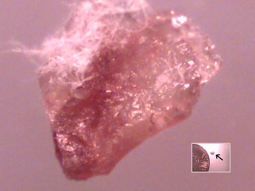
Image 1: sample # 50 at 60x magnification (main),
and at 10x (inset) with penny for size reference.
Circuitry is visible as is the (darker) hermetic feed-through
w/ 90º bend for connection to electrode array
or other component
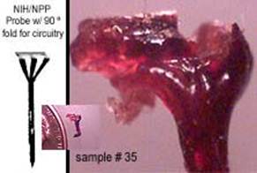
Image 2: sample # 35 compares in size and shape
with probe shown in NIH/NPP documentation.
Integrated circuitry of active probe appears damaged
from structural failure shown here at 60x. This type of
probe has been used by Loeb (and Hambrecht) at the
NINDS.
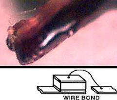
Image 3: Sample # 70 at 60x. A typical wire bond
similar to illustration. The substrate appears to have
an epoxy or polymer coating.
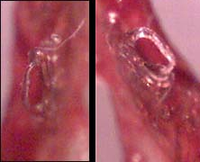
Image 4: Sample # 95 at 60x magnification. Unknown
feature that is definitely fabricated and structured to
serve a purpose. Two views shown.
Summary of Article 1: The photos clearly show something foreign that is not organic mixed with the biological
tissue.
![]()
![]()
![]()
Article 2. - Devices have been analyzed using Energy Dispersive Spectroscopy (EDS):
Energy Dispersive Spectroscopy is a common method used for materials composition analysis and is well
known within the scientific community. I had samples analyzed at Photometrics in Huntington Beach CA.,
which has one of the newer era systems that features light detection ability etc., and confirms the presence
of Silicon in devices which I have recovered. Silicon is the primary and most common material in
semiconductor chips and is not normally present in the body, and in fact is harmful because it contains trace
amounts of arsenic. Additionally, other materials were identified such as Chlorine, which is used in the chip
manufacturing process, Tin, and Aluminum. Some of the data from EDS performed at Photometrics appears
below and complete information is attached to the end of this document.
2.1: EDS Data.4
.jpg)
The data for this sample reads left to right as follows (the
higher the “peak” the higher the concentration of indicated
material): Carbon (C), Oxygen (O), Aluminum (Al), Silicon
(Si), Sulfur (S), Chlorine (Cl), Tin (Sn), Antimony (Sb), and
Iron (Fe)

Sample #15, L to R: Carbon (C), Oxygen (O), Sodium
(Na), Magnesium (Mg), Silicon (Si), Phosphorus (P), Sulfur
(S), Chlorine (Cl), Potassium (K), Calcium (Ca) and (Ca)
again. The sample that produced this result is shown
below at left
This is a photo of sample #15 that showed Silicon and
Chlorine being present. This device doesn’t look as much
like semiconductor as others, but it is and presents an
opportunity to address the oxidization that occurs. The
oxidization that builds up on the implants is a result of an
activated process that occurs when certain metals interface
with the electrolytes present in human tissue, and the
longer the device is implanted, typically, the thicker the
oxidization layer. This is documented in papers and QPR’s
from Loeb. The presence of the oxidization and some
remaining blood and tissue on this device, which was
recovered from my nasal cavity, make it difficult to visually
see semiconductor components, however if you look
closely the circuitry is indeed visible. Note the inset photo
which reveals the actual size of this sample by showing a
penny next to it on the lab slide for reference.
Summary of Article 2: EDS offers proven statistical data that confirms the devices recovered from my person
contain semiconductor material and combined with the visual images provide absolute certain proof that
these devices are foreign and should not be naturally present in my body. Moving forward, what follows will
focus on proving the identity of the individuals responsible for placing them there.
![]()
![]()
![]()
Article 3. - A number of recovered devices show fabrication and design methods which are unique to Joseph
Schulman and/or Gerald Loeb, and are detailed in their U.S. Patent Office filings:
The examples below directly compare images of my recovered devices to images from The US Patent Office
outlining inventions patented by Schulman, Loeb and others within Alfred E. Mann Foundation. It should be
noted that my recovered devices have been implanted for 5 years and obviously will are not in the pristine
condition of a line-drawing illustration, but the design and construction of the recovered devices is similar or
in some cases, identical. From a research perspective, a neural prosthesis needs to remain implanted for
over 40 years to effectively serve a disabled individual, and because not enough research (none in fact,
except for simulations) has been done regarding this, it would make sense for Schulman and Loeb to implant
a variety of devices as well as materials because the continual real-time feedback (or lack there-of) would
allow them to determine which were most effective and also remained biocompatible over time. I have.5
recovered devices appear to utilize a hardened epoxy coating on them as well as others that appear to have
a rubbery type silicone coating. Schulman and Loeb’s patents made during the time of the microstimulator
contract describe much more than a typical “BION” type microstimulator and specifically address alumina,
silicone and epoxy coatings instead of glass or titanium, describe how additional circuitry can upgrade a
device from one which requires an external coil to one that is fully implantable, the creation of electrodes as
small as 15µm using a YAG/UV laser, and one patent even describes how an implntable system can have
it’s components “daisy chained” together by microwire (which is slightly thinner than human hair) rather than
completely assembled inside a glass package. The devices recovered from my person do not all conform to
one design or configuration, and most conform to patent filings of Loeb and Schulman. Some of the
comparisons to those U.S. Patent Office filings follow:
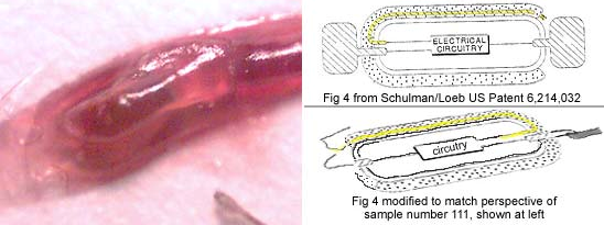
3.1 Sample #111 vs. US Patent 6,214,032 “System for implanting a microstimulator”
Inventors: Gerald Loeb, Frances Richmond Assignee: Advanced Bionics
The image on the left shows my recovered device #111. Patent 6,214,032 on the right (top) illustrates an
invention of Frances Richmond and Gerald Loeb (this same illustration appears in several patents held by
Loeb and Schulman) in which the yellow highlighted path represents encapsulated wire containing electrode
sites that are in addition to the electrodes shown at each end. The lower illustration is modified to show the
invention in the same perspective as my sample #111. In this photo of my sample #111, the circuitry in the
middle of the device is dark and difficult to identify, however the wire bond and path of the wire are clearly
shown and it’s construction is consistent with that of Loeb/Schulman’s filings with the U.S. Patent Office and
further, the documentation shows that “parent case” provisional applications were filed May 29, 1998 for
U.S., and also Internationally on Feb.19, 1997 (within 30 days of my assault).
Continued Next Page…..6
3.2: Sample 110 vs. US Patent 6,205,361 “Implantable expandable multicontact electrodes”
Inventors: Mann/Advanced Bionics
This invention describes an integrated circuit on flexible substrate (so that it will conform to the shape of the
scalp, or muscle etc) with attached electrodes, and is designed to be “folded” into a syringe/hypodermic
needle and injected into the target location. Upon being injected, the electrode array unfolds or “expands” to
an open position. Although this device lists Mann as the inventor, and Advanced Bionics as the assignee,
Gerald Loeb played a role in it’s development as Advanced Bionic’s “Chief Scientist”.

The series of images to the left show my sample #110, and marked-up versions with the blue illustrations showing how
my sample #110 compares to U.S. Patent 6,205,361 for a foldable/expandable array of electrodes. My sample #110 is
consistent with above invention in that: (1) It has three defined areas at one end, and tapers to one section; and (2) it
appears to be on a flexible substrate; and (3) it utilizes a wire perimeter for support.7
3.3 Sample #122 vs. US Patent 6,067,474 “Implantable device with improved battery (capacitor) recharging
and powering configuration” - Inventors: Gerald Loeb, Frances Richmond Assignee: Advanced Bionics
This patent lists Gerald Loeb (as well as F.J. R., also a principal investigator involved with the NIH
microstimulator contract) as the inventors. In sample #122 recovered from my person, a coil (or “antenna”)
can clearly be seen on top of the stack and is represented in the patent drawings as the innermost circle
refrenced as #172
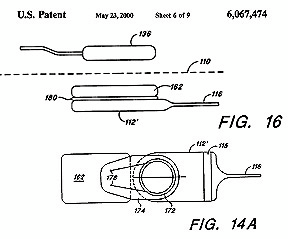
My sample #122 is shown on the left. Patent #6,067,474 is shown to the right an illustrates a microstimulator that uses multiple circuits in a stacked
configuration (with a coil on top, #172 in patent illustration) and the stacking is done to save space, however, such stacking complicates assembly and
lowers yield. Schulman and Loeb claim that no such stacking of chips was performed, nor required by the “BION” microstimulator, however my sample
#122 at left, US Patent #6,067,474, at right, combined with Schulman reporting “unexplainable” low yields throughout his contract
(as low as 30% in QPR#3) should be more than suspicious and immediately prompt inquiry followed by an investigation. And if the above wasn’t
enough, the parent case documentation, U.S. Provisional Application Ser. No. 60/054,480, was filed Aug. 1, 1997 which is during the course of
NIH contract #N01-NS5-2325, and not long after my assault.
Summary of Article 3:
Devices which have been recovered from my person and provent to contain semiconductor material, emulate
and resemble devices which are unique to Joseph Schulman and Gerald Loeb.
![]()
![]()
![]()
Article 4. - Schulman and Loeb file US Patent applications for patient monitoring systems and methods for long
range bi-directional telemetry:
Joseph Schulman and Gerald Loeb have each filed patents as well as later additionas and newer patents for
a “Patient Monitoring System” and “System of Implantable Devices for Monitoring and/or Affecting Body
Parameters” and I contend that the “affecting” part is painful and has been applied by Schulman and Loeb
maliciously through the recovered implanted devices shown in articles 1 and 3 above. What is defined in
these systems is:
•Telemetry using multiple modes or frequencies so that one carrier can transmit a short distance with it
being processed to another capable of longer range telemetry.
•Real time interaction that includes stimulation and recording from the human nervous system
•Audio and video conferencing are integrated into the system that displays the EEG, EMG and other
data allowing Schulman, Loeb and Troyk to simutaneously interact with the system and each other
•A closed loop mode that has a “default” stimulus parameter loaded into memory for each electrode so
that if the subject being monitored breaks the telemetry link, he will still be subject to electrical
stimulation because power can be derived and stored into the capacitor from the Tantalum capacitor-electrode/
bodily tissue electrolyte interface.
My sample #122 is shown on the left. Patent #6,067,474 is shown to the right an illustrates a microstimulator that uses
multiple circuits in a stacked configuration (with a coil on top, #172 in patent illustration) and the stacking is done to save
space, however, such stacking complicates assembly and lowers yield. Schulman and Loeb claim that no such stacking
of chips was performed, nor required by the “BION” microstimulator, however my sample #122 at left, US Patent #
6,067,474, at right, combined with Schulman reporting “unexplainable” low yields throughout his contract (as low as 30%
in QPR#3) should be more than suspicious and immediately prompt inquiry followed by an investigation. And if the above
wasn’t enough, the parent case documentation, U.S. Provisional Application Ser. No. 60/054,480, was filed Aug. 1, 1997
which is during the course of NIH contract #N01-NS5-2325, and not long after my assault..8
Because the illegal and unethical activity of monitoring an unwilling subject involves a database, which one
can assume is backed up and stored somewhere (perhaps even online for remote retreival) and also
involves the program to be housed on a server that can be accessed by Schulman Loeb and Troyk, this
presents considerable evidence that could be obtained by University personnel or law enforcement agencies,
yet unobtainable to me. Because Schulman, Loeb and Troyk participate in this unethical/illegal research both
at home and at work, this creates considerable liability for their employers and those who fund this research.
4.1 - U.S. Patent 6,315,721: “System of implantable devices for monitoring and/or affecting body parameters”
Inventors: Schulman; Joseph H. (Santa Clarita, CA); Assignee: Alfred E. Mann Foundation
(This application is a division of U.S. patent application Ser. No. 09/048,826, now U.S. Pat. No. 6,208,894, and claims the benefit of U.S.
Provisional Application Ser. No. 60/042,447 filed Mar. 27, 1997 and U.S. patent application Ser. No. 09/030,136, now U.S. Pat. No.
6,185,452, which claims the benefit of U.S. Provisional Application Ser. No. 60/039,164 filed Feb. 26, 1997.)
“…a system implemented using multiple communication channels, e.g., a first sonic channel at a first
carrier frequency and a second sonic channel at a second carrier frequency, is also considered to be
within the scope of the present invention…”
4.2 – U.S. Patent 6,208,894: “System of implantable devices for monitoring and/or affecting body parameters”
Inventors: Schulman; Joseph H. (Santa Clarita, CA); Assignee: Alfred E. Mann Foundation
(This application claims the benefit of U.S. Provisional Application Ser. No. 60/042,447 filed Mar. 27, 1997 and U.S. Patent Application
Ser. No. 09/030,106 filed Feb. 25, 1998 which in turn claims the benefit of U.S. Provisional Application Ser. No. 60/039,164 filed Feb.
26, 1997.)
“…A system for monitoring and/or affecting parameters of a patient's body comprised of a system control
unit (SCU) and one or more other devices implanted in the patient's body, i.e., within the envelope
defined by the patient's skin. In accordance with a preferred embodiment, the system operates in closed
loop fashion whereby the commands transmitted by the SCU are dependent, in part, on the content of the
data signals received by the SCU…
… a preferred SCU is also implemented as a device capable of being injected into the patient's body...
Wireless communication between the SCU and the other implanted devices can be implemented in
various ways, e.g., via a modulated sound signal, AC magnetic field, RF signal, or electrical
conduction….In accordance with a further aspect of the invention, the SCU is remotely programmable,
e.g., via wireless means, to interact with the implanted devices according to a treatment regimen …While
the invention herein disclosed has been described by means of specific embodiments and applications
thereof, numerous modifications and variations could be made thereto by those skilled in the art without
departing from the scope of the invention set forth in the claims. For example, a system including multiple
SCUs, e.g., one external and one internal, is considered to be within the scope of the present invention.
Additionally, while the use of a single communication channel for communication between one or more
SCUs and the other implanted devices has been described, a system implemented using multiple
communication channels, e.g., a first sonic channel at a first carrier frequency and a second sonic
channel at a second carrier frequency, is also considered to be within the scope of the present invention
…Transponders, e.g., are devices which can be used to extend the interbody communication range
between stimulators and sensors and other devices, e.g., a clinician's programmer and the patient
control unit. … The clinician's programmer and/or the patient control unit and/or other external control
devices can also communicate with the implanted devices, as described in the parent application,…
Alternatively, such external devices can communicate with the SCU via a transceiver coupled to the
programmable controller. Since, in a preferred operating mode, the signal transmitter and signal receiver
operate using sound means, a separate transceiver which operates using magnetic means is used for
communication with external devices. However, a single transmitter/receiver can be used in place of
transceiver if a common communication means is used..”
4.3 – U. S. Patent: 6,175,764: “Implantable microstimulator system for producing repeatable patterns of
electrical stimulation” Inventors: Loeb; Gerald E. (Kingston, CA); Richmond; Frances J. R. (Kingston, CA)
Assignee: Advanced Bionics Corporation (Sylmar, CA) Appl. No.: 490921 Filed: January 25, 2000
(This application is a Divisional Application of U.S. application Ser. No. 9/077,662, filed May 29, 1998, now U.S. Pat. No. 6,051,017
which application is incorporated herein by reference, and which application was filed in the U.S. under 35 U.S.C. .sctn.371 based on.9
international application number PCT/US97/02576, filed Feb. 19, 1997; which international PCT application claimed priority to U.S.
Provisional Applications Nos. 60/011,870; 60/012,019; 60/011,868; and 60/011,869; all filed Feb. 20, 1996.)
“…Improved implantable microstimulators are covered with a biocompatible polymeric coating… The
microstimulator systems include external control for controlling the operation of the microstimulators. The
control include memory for programming preferred stimulation patterns for later activation by the patient
or caregiver…. can be implanted non-surgically by injection. …upon an external command, or at
predetermined intervals, power and command signals sent from controller cause the various
microstimulators to emit a series of electrical current pulses (i.e., a pulse train) at the desired frequency
and amplitude sufficient to cause the muscles to lift the body for the duration of the pulse train. …also
provides storage and production means for a program of output currents and stimulation pulses that may
then be produced autonomously by the implanted device without requiring the continuous presence of
extra corporeal electronic components, i.e., without the need for an external control device.
4.4 – U.S. Patent 6,164,284: “System of implantable devices for monitoring and/or affecting body
parameters” Inventors: Schulman; Joseph H. (Santa Clarita, CA)
(This application claims the benefit of U.S. Provisional Application No. 60/042,447 filed Mar. 27, 1997 and U.S. patent application Ser.
No. 09/030,106 filed Feb. 25, 1998 entitled "Battery-Powered Patient Implantable Device" which in turn claims the benefit of U.S.
Provisional Application No. 60/039,164 filed Feb. 26, 1997)
“…it is preferably that at least a portion of the program storage be an alterable form
of memory, e.g., RAM, EEPROM, etc., whose contents can be remotely altered as described further
below. However, it is additionally preferable that a portion of the program storage be nonvolatile so
that a default program is always present. The rate at which the program contained within the program
storage is executed is determined by clock, preferably a real time clock that permits tasks to be
scheduled at specified times of day…”
4.5 - U.S. Patent Application 20010054071: “Audio/video conference system for electronic care giving”
Loeb, Gerald E. December 20, 2001
4.6 - U.S. Patent 5,791,344: “Patient monitoring system”
Inventors: Joseph Schulman, A.E. Mann Foundation Appl. No.: 582756 Filed: January 4, 1996
4.7 – U.S. Patent 5,551,016 “Monitoring system and interface apparatus therefor”
Inventors: Loeb; Gerald E. Assignee: Queen's University at Kingston Appl. No.: 084928
“In monitoring systems for acquiring data about a subject, such as are used, for example, in the medical,
scientific and engineering fields, determination of temporal relationships between data acquired from
multiple monitoring devices is facilitated by means of an interface unit which interconnects the
monitoring devices with tape recorders for storing the data and a computer for processing the data.”
Summary Article 4: These systems allow Schulman, Loeb and Troyk to interact with the implanted devices
via radio frequency, and enables this interaction from any location that allows them (Internet access) to
connect to a remote server.
![]()
![]()
![]()
Article 5. - Timing 1:
U.S. Provisional Applications No. 60/039,164 was filed on Feb. 26, 1997 and U.S. Provisional Application
Ser. No. 60/042,447 on Mar. 27, 1997 –
These patent filings pertain to the patient monitoring systems and other technology applicable to a long term
human study and include methods capable of long range bi-directional telemetry.
Summary Article 5: The above patent filings occurred during the same quarter as my assault.10
![]()
![]()
![]()
Article 6. - Timing 2:
Schulman and Loeb report the first functional microstimulators in a QPR just prior to my assault, and report
“tightening up” the accountability and traceability of prototype devices in a QPR following my assault:
“….we were able to demonstrate the feasibility of using a single coil in the microstimulator both to receive
power and data and to act as the tank circuit and antenna for outgoing RF transmission at the same
frequency. The next silicon breadboard is a demonstration of the feasibiliiy and achievable modulation rates
for incoming and outgoing data transmission based on the suspended carrier mode of operation. This will be
done by a chip that records in a shift-register the sequence of detected carrier half-cycles during incoming
RF transmission. The chip then telemeters out that information as a sequence of AM encoded bits….. This
design has passed intensive simulation and is now in layout. Release to the foundry is anticipated in August,
with chips likely to be available for evaluation by early October…” (QPR #5 March 10, 1996 - June 9, 1996)
“In the next quarter, we intend to finalize and validate the sealing process and provide the necessary active
implants to support preclinical chronic animal tests…….” (QPR #7 September 10, 1996 - December 9, 1996)
“During this quarter, we tightened up the traceability and documentation of BION prototype production
units….” (QPR #10 June 10 1997 – Sept 9 1997)
Summary Article 6: This proves that Schulman had achieved functional implants with back telemetry prior to
my assault and that he expressed intent to chronically implant an animal during the following quarter which
corresponds with the date of my assault. Additionally, it shows that following my assault, there was concern
for the accountability of pre-production devices and chips.
![]()
![]()
![]()
7. Schulman has an FCC license (K6BWA) and has 224.840MHz repeaters operating to the North, South and East
of my residence, all within a 22-mile range
An FCC database search reveals that Joseph Schulman holds an “Advanced” class radio license, call sign
K6BWA, and that he upgraded his license as recently as Oct 2001. Evidence shows that repeaters (224.840
MHz) have been arranged in which licenses attributed to Danny Schulman and Barbara Schulman are
involved and their location could facilitate access to the repeater data by Gerald Loeb, James T. Bennett,
and even Phil Troyk. Because Joe Schulman license is used for a repeater in "Hollywood Hills" (yet lives 35
miles North from this location), and Danny Schulman's (lives in Los Angeles) is used for one located in
"Altadena", which is 9 miles from Gerald Loeb, there seems to be some confusion as to where this hardware
is and who can access it. Additionally, Robert Mancini (WB6PRR, note the “W” in call sign) apparently
lives in Oak Lawn, IL (14 miles from Troyk @ IIT), but his license is attributed to another repeater in Altadena
(why two both in Altadena?), this is also more than suspicious. Barbara Schulman will not even admit she is
a radio operator, as attempts to contact here by email result in replies from Joe Schulman. Because Joe
Schulman’s license is attributed to a repeater located in Hollywood Hills, so the repeater at his home or
AEMF in Santa Clarita is operated by Joe under his wife’s license. One interesting observance is that neither
“Sand Canyon”, nor “Hollywood Hills” is a real city, which again, is more than suspicious. Businesses bearing
the name “Hollywood Hills Whatever” (such as Plumbing or Cleaners), are located in zipcode 90027 (which
is Los Angeles, 4 miles from zipcode center to James Bennett’s residence) and “Sand Canyon” is a road in
Santa Clarita that runs past the residence of Joseph Schulman. The tables of information that follow show:
The Repeater Network (Frequency / Call Sign / Location of the Hardware / Status <open or private>)
The FCC Licenses (Callsign / Assignee / Address)
Physical Map of Repeaters (Shows locations of repeaters in relation to my residence).
Private Repeater / Auxiliary Network:
![]()
Freq (MHz) Call Sign Location of Repeater Hardware Status / Mode
224.820 - KJ6JY SANTIAGO PEAK (CONDOR) OPEN
224.840 - K6BWA HOLLYWOOD HILLS PRIVATE
224.840 - KA6UFC SAND CANYON PRIVATE
224.840 - KS6E SHERMAN OAKS PRIVATE
224.840 - KS6K SILVERLAKE, L.A. PRIVATE
224.840 - N6EHD ALTADENA PRIVATE
224.840 - WA6MTM YORBA LINDA PRIVATE
224.840 - WB6PRR ALTADENA PRIVATE
224.860 - N6ENV LA COUNTY FIRE CAMP 49 OPEN
Information above has been confirmed from three sources:
http://www.qsl.net/cora/222_Mhz_Repeater_Guide.htm
http://www.geocities.com/CapeCanaveral/Hangar/6847/
![]()
Identity of above call signs from FCC:
FCC Callsign Lookup www.fcc.gov
Callsign Licensee Name City (according to FCC license)
K6BWA SCHULMAN, JOSEPH H SANTA CLARITA
N6EHD SCHULMAN, DANNY I LOS ANGELES
KA6UFC SCHULMAN, BARBARA L SANTA CLARITA
KS6K LEIDNER, JOEL D LOS ANGELES
KS6E FREEDMAN, MARVIN LOS ANGELES
WB6PRR MANCINI, ROBERT F ALTADENA
![]()
Physical Locations:
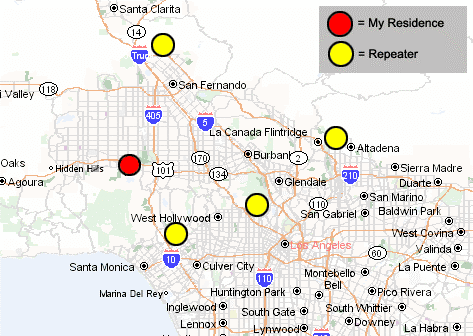
Joseph Schulman’s repeater / auxiliary station locations (*yellow) are shown in relation to my residence (*red) in the map above. Schulman’s RF repeaters are located to the North, South, East, and South East of my residence, all within a 22 mile radius. There is reason to believe Schulman arranged this repeater network through his membership in the ARRL (American Radio Repeater League).
Summary of Article 7: Joe Schulman has repeaters surrounding my residence and their locations do not match that of the licensee’s. Additionally, one of the licensee’s is located 14 miles from Phil Troyk at the Pritzker Institute/IIT. Other repeaters are located near Loeb and Bennett. The repeater locations are more
than just coincidence. Enforcement is needed from the FCC and law enforcement..
![]()
![]()
![]() Update
Update
*Update - I just spoke to Marvin Freedman KS6E at his home. Marvin Freedman told me that “he hasn’t been
active as a HAM for years” and that “I’m not repeating from Sherman Oaks” and “I’m looking at my
equipment,… it’s unplugged, sitting here in Los Angeles”. He also told me that he and Joe Schulman were
“friends”. This suggests that Joe Schulman could be using Marvin Freedman’s FCC license without his
consent”.
Joe Schulman is using his “old friend’s” FCC license for a repeater that is located on or near my Mother’s
property in Encino. He is also using his own license, K6BWA for a repeater that is being operated by James
Bennett located at 2288 Bronson Hill Dr. Los Angeles (aka “Hollywood Hills”), and he is using a license that
he obtained in his wife’s name (his wife would not admit to me that she was a radio operator and insisted I
speak to her husband about it) for a repeater at his residence in Santa Clarita (aka “Sand Canyon”). In fact,
of the six repeaters listed in the table below, 3 are in non-existant cities (Hollywood Hills, Sand Canyon and
Silverlake are not real cities with no US zip code). Joe Schulman is using this radio signal to control
biomedical sensors which is part of his work at the Alfred E. Mann Foundation ( http://www.aemf.org/ ) which
developed sensors called the “BION”, ( http://ami.usc.edu/Projects/Bion/media.asp or
MicrostimulatorsAndMicrotransducersForFunctionalNeuromuscularStimulation%20
7NS52325.pdf
Marvin Freedman lives in Los Angeles and can be contacted below:
Marvin Freedman KS6E 310-470-1116
![]()
![]()
![]()
8. Professor Wise from Univ. of Michigan reports in a QPR that because of bandwidth and impedance issues,
200MHz should be chosen for remote, wireless stimulation using a neural prosthesis
As if articles 1 through 4 were not enough evidence to prompt action, further evidence of the repeaters use is
the frequency Joseph Schulman’s repeater/auxiliary stations are operating at (224.840 MHz). The
significance of this is best explained by Professor Kensall D. Wise, University of Michigan, respected for his
many years and considerable contributions to the NINDS/NPP:
“…the most important issue of an implanted biotelemetry system is power dissipation. To minimize the
power of a transmitter, we have to select the lowest practical RF carrier frequency, since RF circuits
dissipate power that is proportional to their operating frequency. The FCC has authorized unlicensed use of
the 38-41MHz, 88-108MHz, and 174-216MHz Very High Frequency (VHF) bands for Industrial, Scientific
and Medical (ISM) telemetry purposes. Other bands in the microwave region (900MHz and above) are not
considered because of high tissue absorption at those frequencies. On the other hand, a higher carrier
frequency is desired for wider bandwidth in data transmission. As the result of these trade-offs, 200MHz is
chosen as the carrier frequency…” (recent QPR #5, (Oct/Dec 2001) Contract NO1-NS-0-2329 “Thin-Film
Intracortical Recording Electrodes)
Ken Wise has been involved with the NPP and using micromachined Silicon electrodes to stimulate and
record from the nervous sytem since as early as 1992, and is obviously very accomplished and
knowledgable. In the above, he establishes 200MHz as the preferred carrier frequency because higher
frequencies use too much power, and lower frequencies do not penetrate the impedance of the tissue as well
as higher frequencies.
Summary Article 8: If someone wanted to use wireless radio frequency to stimulate and record from an
unwilling human participant, a frequency near 200 MHz would be desired.13
![]()
![]()
![]()
9. Schulman reported acquiring an ISDN “Connectix” phone as part of contract #N01-NS5-2325 claiming it would
be used for file sharing and later, a company he founded called “NeuroDyne” markets a new system which used
such an ISDN video-phone to enable multiple physicians to tele-conference while analyzing a patients
biofeedback signals
In QPR #5 (March 10, 1996 - June 9, 1996), Schulman reports:
“In order to facilitate communication between the Mann Foundation (Schulman) and Queens University
(Loeb), an ISDN telephone line and high speed modem have been installed with service to the Internet.
The Connectix VideoPhone system is in use and remote file access and terminal sessions will soon be
available between engineering and documentation computers at both locations…”
This ISDN video phone was actually used to provide real-time bio-feedback data from Schulman in Valencia
CA, to Loeb at Queens University, and allow them to conference and interact while monitoring me and the
biofeedback from their microstimulators during this unethical and illegal research. They also based parts of
their “patient monitoring system” patents on this. The fact that Schulman and Loeb used the Connectix
Phone for more than “remote file access” is substantiated by this press release from NeuroDyne, a
corporation founded by (not a coincidence) it’s President, Joseph Schulman:
![]()
NeuroDyne/E-Tech Press Release:
August, 1999: A new Internet technology will allow a patient to carry on a face-to-face conversation with a
doctor who is a few miles or even thousands of miles away while his physiological measures, such as EKG,
EEG, EMG, GSR etc. are displayed in real-time on the doctor's screen for assessment... the ability for
healthcare colleagues and specialists several thousand miles apart to conference concerning a patient,
while interacting via audio, video and active monitoring of the patient's physiology.… Optionally, a Video
Camera, VoxPhone software, and an Internet connection, allow two individuals virtually anywhere in the
world to carry out a private conversation or to support a conference with up to five individuals. Under the
joint venture, the VoxPhone interface will be expanded to allow the transfer of real-time data from
NeuroDyne Medical's biomonitoring instrumentation in addition to voice and video information. This
physiological information can then be displayed graphically on both computer screens as well as being
saved for further analysis…….”
Summary Article 9: It is becoming obvious (it it isn’t already), that Schulman and Loeb are guilty of my
allegations. They implanted these microstimulators using a syringe leaving virtually no externally visible
evidence and they expect you and others not to believe it because “it sounds crazy”. You don’t have to
believe me but you do have to believe the evidence. The evidence is far too much and too convincing to be
“amazing coincidence”. All of the evidence presented is documented, factual and proven. No speculation or
fabricated conclusions. Just fact. This is currently page 15 of about 50 and the evidence in the following
pages don’t make Schulman and Loeb look any more innocent. That is because they are not.
![]()
![]()
![]()
10. Schulman reports a “faulty” diode and resistor required that they be removed in-house and replaced,
however the patents of Schulman, Loeb and Troyk allow diodes and resistors to be eliminated by integrating a
chip based on the suspended carrier telemetry protocol resulting in a smaller device package size.
Schulman reports vendor errors have required a diode and resistor to be cut from the chip (removed) and
then replaced. It is specifically indicated that these components were “defective” and that they would be.14
replaced with two new (off the shelf) surface components and that doing so required in-house post-processing.
The legitimate reason behind elimination of the resistor and diode involves Schulman’s want and
need for a smaller implant, so placing tiny additional circuitry with the implanted chip would be needed and
thus, also would need to be explained. I contend that the components were not defective and that they were
not replaced with two comparable components as indicated. The reason Schulman removed them is
because the diode and resistor would not be necessary after stacking an additional, small circuitry, (based
on the Suspended Carrier telemetry protocol) onto the existing ASIC as described above. This additional
circuitry was for the mixed signal demodulation required for long-range RF bi-directional telemetry and also
performed DAC, clock, state machine and other functions. Schulman lays it on thick in QPR’s, however
contradicting (but accurate) explanation exists in their patent filings where they are forced to be honest in
order to protect their invention:
QPR #3 conceals the reason for removing the diode and resistor by claiming the components are defective:
“…we were dealing with a chip that had a defective diode on board, which made the chip useless. Luckily,
the position of the diode in the circuit and physically on the chip was such that it could be effectively
removed from the chip and replaced by an external diode. Moreover, the resistor, essential for the data
demodulation, was also conveniently placed and could be replaced by an external device. Having two
additional devices in a small package required redesign of the package which in turn demanded
repositioning of the bonding pads using a relatively inexpensive gold-bumping process…” (QPR #3, Sept
10, 1995 – Dec 9, 1995)
In the patent below, Schulman describes how additional circuitry can be used to upgrade an implant device
from a system that requires an external coil and driver circuitry, to one that is fully implantable. One doesn’t
have to look far past contract #N01-NS5-2325 when wondering how Joseph Schulman came up with such a
concept. Other descriptions in U.S. Patent 6,067,474 have allowed me to assess that Schulman and Loeb
refer to the system used for their illegal and unethical research as a “proximity system” and that it was
developed as part of NIH microstimulator contract N01-NS5-2325 and substantiated by it’s filing date.
“Appropriate switching circuitry is included with the battery (or capacitor) in the second device to convert
the dc power of the battery to ac power for transmission to the first device. This ac power may be
modulated, as desired, to also transmit information, e.g., control signals, from the second device to the first
device. Yet a further embodiment of the invention, hereafter referred to as the "proximity system"
embodiment, resides in a fully implantable system that includes first and second implantable devices. The
first device houses electronic circuitry for performing a desired function. The second device houses a
replenishable power source, and may also include additional circuitry. Thus, one use of this proximity
system embodiment allows a second device.. that has heretofore been included in an external device, to be
implanted proximate an implant device of an existing system, thereby effectively upgrading the existing
system to a fully implantable system.” (6,067,474: “Implantable device with improved battery recharging
and powering configuration” Inventors: Joseph Schulman (U.S. Provisional Application Ser. No.
60/054,480, filed Aug. 1, 1997)
U.S. Patent Office filing contains accurate information:
Patent 5,697,076: “Suspended carrier modulation of high-Q transmitters” (the only patent
legitimately indicating that it was made under government support) December 9, 1997, Inventors:
Troyk; Philip R.; Heetderks; William; Schwan; Martin; Loeb; Gerald Assignee: Illinois Institute of
Technology (Chicago, IL); United States of America as represented by the Department of Health
and Human Services (Washington, DC) Appl. No.: 432605 Filed: May 1, 1995.
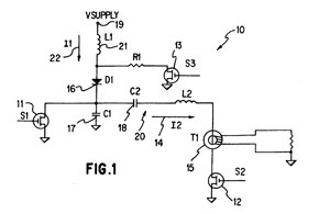
“…When switch 13 is closed, current 22 rises to (Vsupply/R1) with an R1/L1 time constant. Thus, with the
proper choice of R1, if switch 13 is closed long enough in advance of the closing of switch 12 (restart), the
proper initial condition for current 22 can be achieved. When switch 12 is closed and Class E operation
resumes, switch 13 opens, causing current 22 to flow into diode 16 instead of R1.
…Elimination of the R1-S3 branch may be possible with an appropriately sized choke inductor 21. In this
case, the current 22 is allowed to go to zero, even for "short" off periods.”
The above diagram is from their patent and obviously shows accurate information. The diagram that follows
however, from NIH QPR #10 contains less “precise” information and further conceals how suspended carrier
was being used during contract #N01-NS5-2325 :
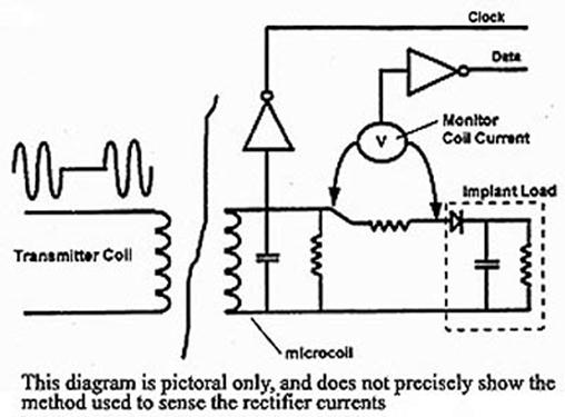
“Not precisely” isn’t even truthful because the truth would read “not even close”
The patent filing below shows how diode and resistance are present in the circuit diagram, but are not
represented by actual components:.16
U.S. Patent 6,035,237: “Implantable stimulator that prevents DC current flow without the use of
discrete output coupling capacitors”
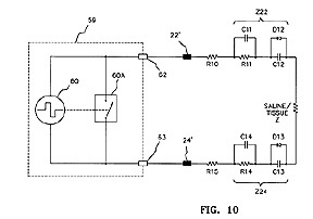
“As illustrated in FIG. 10, the coupling capacitor is actually formed by using the electrode-saline interface
that results when a conductive electrode comes in contact with saline body fluids. In FIG. 10, Z24
represents the complex impedance between electrode 24 and the saline. Capacitor C12 and diode D12
(as well as capacitor C13 and diode D13) represent the passivation or oxide insulation layer that exists at
the surface of each stimulating electrode.”
In this invention, the result of the oxide insulation layer functions as a capacitor and diode, so although the
circuit layout shows a diode, there is only oxide build-up that causes some resistance and capacitance and
no true hardware components.
There is no mention of chip stacking in the text body of contract QPR’s and when Schulman finally reports
using a chip allowing elimination of the diode and resistor (which ironically doesn’t happen until the final QPR
in 1999), the additional circuitry is showed next to the existing circuitry in a planar configuration. This poses
the following question: If no chip stacking occurred, what is meant in the text header contained in QPR #2
following subject header “Work at the Alfred E. Mann Foundation” that reads as follows:
3. Electronic assembly, stacked chips, side by side chips
“As reported in the 1st Progress report of this Contract, a plan was developed to rework the
microstimulator integrated circuit wafers which had been fabricated at the end of the first microstimulator
NIH contract. That circuit was not fully functional due to problems associated with the on-the-chip
demodulation l rectifier diode……”
Additionally, if no chip stacking was used for the BION microstimulator, what was the cause for the
abnormally low yield of microstimulators which was consistenly around 30%? The “Evidence Detail” section
of this document has shown a stacked chip device recovered from my person and Schulman’s patents also
describe a stacked chip configuartion, most of which were initially filed during the microstimulator contracts
period. Although Schulman eventually revealed the method of additional circuitry that was capable of
eliminating the diode and resistor, the added chip was shown in a planar configuration rather than stacked
which requires more substrate area. He concealed this throughout the duration of the contract and only
partially revealed it in ironically, the final QPR of the contract in 1999. His U.S. Patent applications prove that
he was aware of and practicing this invention as early as 1995 and the QPR’s during the four years of the
contract never mention fixing the chip design so as not to necessitate the addition of replacement
components which suggests that this method of adding additional circuitry was occurring for the duration of
the contract beginning with QPR1 in 1995 when he reported a need to cut “faulty” diodes from the chip. The
final QPR from 1999 offers an illustration which shows one simple chip added next to (not stacked) the
existing circuitry:.
“…we revised the rectifier/data demodulator of MOS8 for integration with existing 2MHz microstimulator
circuitry. The existing external diode, amplitude demodulator, and clock recovery circuit were replaced by a
new ASIC cell that uses the techniques of MOS8. (Images 10 and 11, above) Presently these chips are
under test…”
It is reported that the above ASIC “cell”, which finally solves the 4 year old resistor/diode problem “uses
techniques” of MOS8. I contend that this “cell” exists on a ASIC design layout that was submitted during the
first year of the contract and that Schulman waited until the final QPR#16 to reveal it. This cell could have
been present on (and cut from) any number of the early wafer/chip runs that he falsely reported being
“unusable”.
It is reported multiple times that a “faulty” diode needed to be replaced and is shown again in this instance:
“A major effort was expended dealing with the new microstimulator development and in correcting silicon
foundry errors via chip microsurgery …a new corrected layout was sent to the foundry for another run of
wafers… when the wafers returned, it was observed that they did not work …the design rules provided by
the foundry allowed the shorts …by cutting a trace on the integrated circuit, the external diode could be
reliably removed. A diode-resistor combination could then substitute for the defective on-chip
components.” - Schulman/Loeb/Troyk QPR#1 – March 10, 1995 – June 9, 1995
Again, patent documentation makes argument against Schulman’s reporting, and here he describes how
removal of components followed by adding additional small circuitry can actually result in a smaller overall
package:
Patent 6,035,237: “Implantable stimulator that prevents DC current flow without the use of discrete output
coupling capacitors”
“The implantable stimulator of claim 3 wherein said first and second circuit means are realized using
CMOS transistors configured to function as prescribed circuit elements on the same semiconductor chip
…while such DSP circuitry may utilize a significant number of CMOS transistors, configured into
appropriate processing and logic circuitry, the overall space required by such DSP or other circuitry on
the chip, or a supplemental chip, particularly given the smaller trace sizes associated with modern CMOS
devices (0.8 micron and smaller) could still be less than using discrete coupling capacitors (resistor)..18
The repositioning of the bond pads was done to create electrical contacts for attaching the additional
suspended carrier/long-range telemetry circuitry which also allowed the elimination of diode/resistor. This
activity is not revealed in NIH QPR’s, because Shulman claims that the additional bond pads were needed to
attatch the diode and resistor which was cut off of the original chip. Further evidence can be found in U.S.
Patents 6,315,721 and 6,164,284 which describe the following:
“…The SCU 302 is primarily comprised of (1) a housing, preferably sealed and configured for
implantation beneath the skin of the patient's body as described in the parent application in reference to
the implanted devices, (2) a signal transmitter in the housing for transmitting command signals, (3) a
signal receiver in the housing for receiving status signals, and a programmable controller, e.g., a
microcontroller or state machine…”
The “state machine” mentioned above is included in the additional circuitry that Schulman used which
allowed the elimination of the resistor and diode
“…For example, sensor circuitry can be coupled to the electrodes …and provided the sensed data to the
controller circuitry. Preferably, the sensor circuitry includes a programmable bandpass filter and an
analog to digital (A/D) converter that can sense and accordingly convert the voltage levels across the
electrodes into a digital quantity. Alternatively, the sensor circuitry can include one or more sense
amplifiers to determine if the measured voltage exceeds a threshold voltage value or is within a specified
voltage range. Furthermore, the sensor circuitry can be configurable to include integration circuitry to
further process the sensed voltage. The operation modes of the sensor circuitry is remotely
programmable via the devices communication interface…”
The programmable bandpass filter is also part of the additional circuitry that Schulman integrated after
eliminating the diode and resistor during his NIH contract and the additional functionality of the added
circuitry enabled bi-directional telemetry over greater distances than with a normal inductively coupled link. In
order to sense and monitor as described above in patent text, and also the ability to do so with only 2-5%
modulation and switch in 4 clock cycles or less which is described in Schulman’s QPR’s, the “sensor
circuitry” mentioned above must be implanted with (onto or next to) the microstimulator. This is in contrast to
a typical inductive link where this sensing and monitoring takes place between a coil attached outside the
skin and an implanted device where the impedance of the tissue and the increased distance do not allow the
low modulation and instantaneous switching. Although much of this evidence pertains to Schulman and
Loeb, Phil Troyk worked very closely with them on the Suspended Carrier chip, the back telemetry and also
the overall packaging. The fact that it is reported that Martin Schwan performed the removal of diodes and
resistors at IIT also suggests that both Troyk and Schwan direct knowledge of Schulman and Loeb’s intent
with the device. In email correspondence, Phil Troyk responds to my inquiry about addition of the small
circuitry by denying any intent for it to be added to the implanted package and claimed that it was to exist
outside the skin, but then in an about face, claims that the idea was “one of the other team members” and
that he “saw no benefit to it”. This email correspondence is attached at the end of this document.
Summary Article 10: Respected Investigators, Professors and Scientists are capable of telling lies, they do
tell lies, and Schulman has told more than his share. The diode and resistor were not defective. They just
needed the additional circuitry integrated / added into or onto the implanted portion.
![]()
![]()
![]()
11. In a table of data listing the specs for components of the “BION” microstimulator, Schulman indicates that
the diode used in replacement of the “faulty” diode is a “THD9064”, however there doesn’t appear to be any
such diode in existence.
In QPR #2 (June 10, 1995 - Sept 9, 1995), a table of “Specifications” is present that provides details
regarding each of the “BION” microstimulator components and indicates a mystery diode. Additionally, a
table of “Suppliers” lists an undetermined vendor for an unknown component.
Suppliers:
1. Kimbel Borosilicate Glass.19
2. AVX Tantalum Corp
3. Vendor to be selected by A.E. Mann Foundation
Specifications:
Part Abbrev Specification
Glass Capillary cap 0.079” OD
Glass Bead bd 0.015” ID 0.065 OD
Iridium Ball Ir ball 0.065” OD
Diode D THD 9064
Integrated Circuit Chip IC chip 3 micron, double poly, CMOS
1. THD 9064 does not appear to be a commercially available diode. The fact that no such “THD9064” diode
exists should alone prove that Schulman eliminated the diode rather than replaced it and the false data
above is reason for Alan Price and John Krueger at the Office of Research Integrity to find Schulman guilty of
misconduct and because he didn’t act alone, the other Investigators should be subject to diciplinary
measures as well.
2. A search for THD 9064 on two popular search engines (Hotbot and Google using the terms diode thd
9064 in various forms) returns a total of 3 results: (1) New Focus 12-GHz Amplified Free-Space
Photoreceiver (which uses a MEMS class 25µm schottky diode), (2) Siemens SDA9064-5 Digital Deflection
MicroController (frequency doubler), and (3) another microcontroller from ICS.
![]()
![]()
![]()
12. Throughout contract #N01-NS5-2325, Joseph Schulman fabricates an absurd amount of “vendor error” and
“faulty product” which was done to conceal the real reason for the excessively low yield of microstimulators
which can be attributed to the error prone stacking process of the smaller unethical implants
“Yield of the microstimulators after winding is approximately 30%. The reason for this poor yield is not yet
known. The integrated circuits have been pretested. In some of the defective stimulators, measurements
show that the external diode and resistor are not properly connected. In others the precise cause is
unknown. Presently, test fixtures are under development, at the Mann Foundation, to permit testing of the
electronic module at all assembly levels.” (Contract N01-NS5-2325 QPR#3)
This atrocious yield of 30% is factual evidence and should have flagged concern upon NIH review. For those
not totally familiar regarding ASIC fabrication process, a brief explanation may help. When Schulman says
the circuits have been pretested, this is pretty understandable as testing a single IC after production is a
simple process. The window of consistency for yield of chips from foundry runs industry wide (in process
sizes ranging from .05µ to 3.0µ, CMOS or BiCMOS) is always in excess of 96% and is typically approaches
99%, which means there is very little “vendor error”. Schulman indicates that after he gets his hands on
them, yield falls to 30% and struggles to explain, but indicates that the problem is “unknown”, but “some” of
the problem is that the diode and resistor replacing the “faulty” components that were removed at IIT are not
“properly connected”. The “BION” microstimulator documented in this contract does not stack circuits in a
vertical or 3D fashion and attaching basic components to bond pads in a 3.0µ or 1.5µ CMOS process is not
immensely difficult, especially when you take into account the experience of Mann personnel who have prior
experience with smaller chip processes used in cochlear implants and at IIT who is a leader in MEMS scale
and Nano scale fabrication. There is another reason for 70% of the finished product being non-functional and
the problem is not “unknown”, it is deception that Schulman must conceal because the only legitimate
explanation for this poor yield is that the chips were being stacked in order add functionality (long range
telemetry) and save space and a quantity were being misappropriated as well..20
Here a “clerical error” causes open pads, however open pads such as these would be beneficial if your intent
was to dice and stack the chip:
“Among the chips included on the wafer run was a test chip for the suspended carrier front end. Due to a
clerical error in the process of combining the chips onto one reticule, that test chip had open circuits at
many of the pads, making testing of the chip essentially impossible. These opens and any other problems
which can be fixed with metal layer changes will be corrected on the wafers which have been held in the
early stages of processing. As this report is being prepared for submittal, the corrections in the metal
layers have been submitted for two more wafer releases.” (QPR #15)
In this quarter, Schulman blames Slicex, a vendor in Salt Lake for two different errors and claims an entire
run of chips are useless
“Prior to delivery of the chips it was discovered that an unfortunate error existed in the layout at the upper-most
cell level. A long strip of via/contact had been placed, by Slicex, across the entire length of the
repeater chip rendering it inoperative. Equally unfortunate was the substitution of cells from an earlier
revision of the layouts in the test chip. Therefore neither of these chips were functional upon delivery.
Fortunately, some of the circuits used in the Repeater chip design had been included in another MOSIS
submission as part of work on ITT's contract: Multichannel Transcutaneous Cortical Stimulation System.
Therefore we were able to use that chip, MOS2, to test the power supply regulator, and rectifier/data
decoder Both of these circuits are key components for the telemetry of the proposed micromodules” (QPR
#10)
E-mail correspondence with Tom Wolf, President of Slicex, reveals conflicting information:
Mr. Wolf writes: “…We brought Dr. Huber in primarily to address the latch up problem as AEM (Alfred E
Mann Institute) was pushing the IC process beyond its ability… Dr. Schulman wanted to use an entire
reticule which meant we placed 5 IC's in a stack, and then 2 IC's rotated 90 degrees at the end. At this
point, the industry did not have good tools for debugging multiple IC's on a reticule (I am not sure if this
is possible even today). But at that point, the only way to check was with the human eye. Shortly after
the IC came back and was deemed acceptable by Schulman, I visited Schulman at AEM. He expressed his
satisfaction with our work and then introduced me to Ron Liebel of MiniMed. He told Ron that he should
use us and that we were great, just expensive. After which, we helped MiniMed with their artificial
pancreas chip. At this point Dr. Schulman stated he had lots of new work for us, but we never saw any
more from him. Just his sister companies, MiniMed and ABC (ABC = Advanced Bionics Corp) Now at ABC,
we did several million dollars worth of business. I don't understand that Schulman could say we didn't
understand anything, when we designed 1 IC for him that worked and 17 for ABC. Especially since
according to Schulman, the only IC that had worked first time for AEM up until that point in time was the
one done by SliceX….
In email correspondence between Joseph Schulman and myself, a different scenario is portrayed:
“I WAS CONCERNED BECAUSE THEY ALL SAT QUIETLY AND DIDN'T ASK ANY QUESTIONS, AND
WHEN I ASKED THEM IF THEY WERE SURE THEY UNDERSTOOD ALL THE SCHEMATICS WE WERE
DISCUSSING THEY WOULD ALWAYS ANSWERE YES. FINALLY WHEN THEY PRODUCED THE CHIPS, IT
WAS OBVIOUS THAT THEY DIDN'T UNDERSTAND ANYTHING AND THUS HAD MANY ERRORS IN THE
LAYOUT. WHEN I POINTED OUT THE ERRORS TO THEIR MANAGEMENT, THEY PROMPTLY RETURNED
THE FUNDS WE PAID THEM. ANOTHER COMPANY THAT WORKED WITH THEM LOST OVER A MILLION
DOLLARS DUE TO THEIR SCREWUPS…”
Mr. Wolf mentions that Schulman was stacking a full reticule as well as “pushing the process beyond it’s
ability” which indicates that the design was sacrificing reliability in favor of a smaller chip size. If this chip
were just being used for the BION, space savings should not have been a concern as this chip was in a
1.5µm process which is considerably smaller than the 3.0µm chip that the project began using initially and as
shown below in another section, there is enough room inside the BION glass capsule for circuitry and this is
definitely not an issue. Although Mr. Wolf does admit some troubles with the full reticule, he indicates that he.
is certain that Slicex is not responsible for an entire run of chips being non-functional and that they provided
Schulman and AE Mann with a working design.
Summary Article 12: There are far more instances than what I report here. Schulman was keeping some of
the chips for the smaller devices and was forced to cover this up by saying yield was poor and vendors made
mistakes.
![]()
![]()
![]()
13. Other Evidence
Much further evidence exists in Joseph Schulman and Gerald Loeb’s U.S. Patent Office filings and the
Quarterly Progress Reports from contract #N01-NS5-2325. This evidence shows fraudulent reporting, that
technology and alternative implantable device invention discoveries occurred during the contract period, and
also provides insight regarding motive and other factual evidence. Most evident however is that many of the
inventions and methods involve integrating or stacking additional circuitry allowing smaller implant sizes and
the ability to eliminate external components and increase the range and options for bi-directional telemetry,
and also making it possible to pursue the unethical long term research involving an unwilling subject.
Previously, in article 12, Mr. Wolf from Slicex reports that “Dr. Schulman wanted to use an entire reticule
which meant we placed 5 IC's in a stack, and then 2 IC's rotated 90 degrees at the end”. The following
shows an illustration from Philip Troyk’s separate NIH contract for a visual prosthesis as well as text from
those QPR’s:
“….the NPP is highly motivated to initiate the development of a fully implantable cortical stimulation system
which could be used to provide inputs and computer control for hundreds, to over one thousand, implanted
cortical electrodes. This project used the combined capability four organizations, the Illinois Institute of
Technology, …., and the A.E. Mann Foundation. The device specified and designed in this contract has
significantly higher packaging and functional density (is smaller) than any other implantable neural prosthesis
previously developed.”
Stacked visual prosthesis chips with portion rotated 90 degrees
Individuals at the Mann Foundation have expressed a desire to create a “universal family” of
microstimulators that could be used for a visual, auditory or motor prosthesis. Such a universal device would
have to be much smaller than the “BION” developed under contract #N01-NS5-2325 and be flexible so as to
conform and stretch in response to it’s implanted environment. The evidence presented here suggests that
Schulman began development of this universal device using NIH grant funding from #N01-NS5-2325 and
fundamentals learned are applied today by Mann Corporate ventures Advanced Bionics and Second Sight.
“Work at the Alfred E Mann Foundation is increasingly directed towards a medium to large scale
manufacturing of microstimulators. Methods are being developed for reliable and reproducible
manufacturing procedures that can utilize batch-processes rather than production steps on an individual
basis” (Schulman, QPR #3)
Later, from R. Greenberg, NC retinal chip investigator and now President of Mann founded “Second Sight”
“Also, by splitting the chips up into smaller components, and utilizing techniques such as solder bumping to
connect the chips with flexible electrode substrates, we shall keep the sizes to a minimum….” (Robert
Greenberg Mann Foundation Multiple-Unit Artificial Retina Chipset System To Benefit The Visually
Impaired)
Most recently from USC media:
“Health & Medicine – USC News;
…developing an eye chip that would be placed in the retina and restore some vision to people with
degenerative diseases. The intraocular retinal prosthesis is created through microelectronics. The eye
chips will be manufactured by Second Sight, a company that was founded by Alfred E. Mann, the Chair of
the Board of Directors of the Alfred E. Mann Institute for Biomedical Research at USC
http://www.usc.edu/student-affairs/dt/V144/N26/04-doctor.26c.html
Schulman defines smaller devices in patent applications with descriptions far smaller than the “BION”. At 25
mils total thickness, this is approx 1mm, and thus many times more compact than the BION.
“…A thin hermetically sealed electrical feedthrough suitable for implantation within living tissue permits
electrical connection between electronic circuits sealed within an hermetically sealed case and electrical
terminals or contacts on the outside of the case …For example, using currently known processing
techniques, the frame and lid can be as thin as approximately 4 mils. The height of the cavity can be as
small as about between 5 to 10 mils depending on the connections of the electronics contained within the
cavity. The insulating layers, as indicated above, can be on the order of less than 1 mil thick, it is thus
feasible using presently available processing techniques to construct an implantable device less than 25
mils thick, yet still providing an hermetically sealed case and hermetic feedthroughs.” (U.S. Patent
5,750,926: “Hermetically sealed electrical feedthrough for use with implantable electronic devices”
Inventors: Joseph Schulman Filed: Aug 16, 1995)
6,067,474: “Implantable device with improved battery recharging and powering configuration”
“Although the preferred power source for use within the fully implantable systems described herein is a
rechargeable battery, it is to be understood that other power sources may also be employed. For
example, an ultracapacitor (also known as a supercapacitor) may be used.. Thus, for this type of
application, where recharging must occur on a regular basis, and when appropriate discharge circuits are
employed to control the rate of discharge or energy withdrawal, the ultracapacitor provides a viable
alternative to a rechargeable battery for use within the implantable system.”
Patent 5,522,865 “Voltage/current control system for a human tissue stimulator”
Multiple Chip Control: “In the preferred embodiments thus far described, the ICS comprises a single chip.
However, multiple chips of the same or similar circuitry may be usefully employed in a human tissue
stimulator. In such an embodiment, a circuit at the input of each chip permits the interconnection of
several chips into one functional unit by making one of the chips a master device which receives data and
clock signals and then distributes such signals to all the slave chips. In this manner a large number of
chips may be connected together forming a system with a large number of output channels”
Chips too big?.
“To provide an easier fit in the small Microstimulator package, the chips must be lapped from a thickness
of about 500 microns down to under 200 microns. While this can be done on individual chips, it is much
easier (and more economical) to do it on an entire wafer before it is diced into individual chips. As
mentioned in the previous report, an additional passivation layer (probably silicon nitride) is needed to
protect the chips from damage due to the attached ferrites.” (QPR #6)
Schulman reports above that post-processing is needed to get the chips thin enough to fit into the
microstimulator package, however there appears to be ample room within the glass housing for the tiny 1.5µ
and 3.0µ process chips of the BION. A photo of an early and more recent BION is shown below:
Summary
Joseph Schulman and Gerald Loeb have both acted irresponsibly, selfishly and have caused me
considerable pain, suffering and other damages during the last 5 years. They have anticipated that no proof
would exist of their crimes and that nobody would believe a story of this nature. This will no longer be
possible as the evidence and cause for investigation is presented here and now. Loeb’s plans for the future
at USC-AMI show a new improved version of the “Connectix” Video Phone mentioned as Article 9 in the
“Evidence Detail” section above, however in this embodiment the server for this criminal misconduct will
remain on campus allowing Schulman and Loeb to record data from and stimulate their unfortunate research
subjects who are unwilling recipients of microstimulators, whether at home, on campus, on vacation, or at a
National conference or event by remotely accessing the university “Telemedicine” server from their location.
I’m certain that Mr. Steven Sample, President of USC did not anticipate this kind of trouble when welcoming
the Alfred Mann Institute to USC, and had he known, he may have reconsidered, because this kind of human
research misconduct far exceeds any that has existed, even at Johns Hopkins, whose Biomedical Dept has
also received Mann funding. Loeb’s future plans and ulterior motive for developing tele-medicine technology
are a liability for USC and should not be allowed to continue regardless of revenue or finances, because this
is a losing proposition no matter how you look at it.
Loeb’s newest invention for USC is as follows: United States Patent Application 20010054071
Inventors: Loeb, Gerald E.; (Los Angeles, CA)
“ …audio/video-call system allows communication using audio, video and/or data. The system includes two
communication systems--one for the user and one for the caregiver. Each communication system includes
a console coupled to a television. The console has a digital processor, storage, software, and connections
to telephone equipment, channel tuner, a video camera, and steering for the video camera. A remote
control issues commands to the console to initiate or accept calls to the other communication system. The
phone line is used to carry the audio portion of the call while the network is used to carry any video and/or
data portion of the call. In some embodiments, a passkey allows the caregiver's communication system to
control the user's communication system without any interaction by the user. In other embodiments, more
than one video camera is used for a communication system. A microphone can be coupled to the remote
control to collect the audio channel for the call…”.
In conclusion, I hope that everyone who reads this will do what he or she can to ensure this behavior is
discontinued and that disciplinary measures are pursued. I cannot take the law into my own hands. I need
your assistance resolving this. I am willing to cooperate in any fashion that will assist authorities in realizing
the truth regarding this situation and this would include having these devices analyzed using techniques or
methods that are available which I cannot currently arrange due to financial reasons. Thank you for your
assistance regarding this manner.
Attachments
1. Additional recovered device images
2. Glossary
3. Recovered device materials analysis documentation and data from Photometrics
4. N01-NS5-2325, titled “Implantable Microstimulators and Transducers for FES”
5. N01-NS-7-2365 titled “Multi-Channel Transcutaneous Cortical Stimulation System”.
6. E-mail correspondence
More images of devices recovered from my person are presented here. Despite the overwhelming evidence
presented above, these devices will make the strongest case against Joseph Schulman and Gerald Loeb
and cannot be ignored.
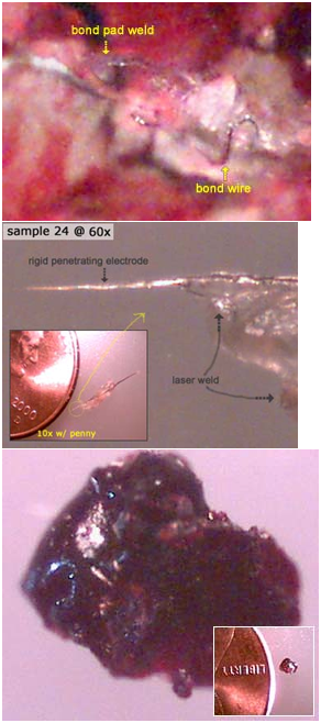
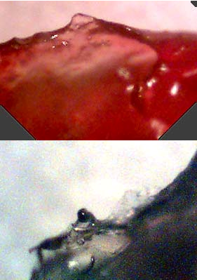
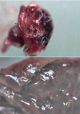
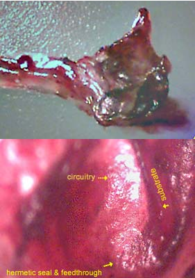
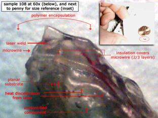
There is a reason why these devices look the way they do. The first reason for their appearance is that they
have been implanted for 5 years. The second is that if they were to be recovered, Schulman and Loeb would
not want you to recognize them, and the third reason is explained by Jerry Loeb himself:
“Therefore, modification of the microstimulators' chemical nature and/or superficial physical contours to
avoid, prevent and/or discourage an immunological response by the body, would be advantageous.”
![]()
![]()
![]()
Glossary.
Glossary links on the Internet:
Everything: http://whatis.techtarget.com/whome/0,,sid9,00.html
Semiconductor: http://semiconductorglossary.com/
Medical: http://www.medicinenet.com/script/main/AlphaIdx.asp?li=MNI&p=A_DICT
AEMF: Alfred E. Mann Foundation
ASIC: Application Specific Integrated Circuit
ARPA: a way universities have of saying “DARPA” (since when has “defense” become a dirty?)
BiCMOS: Complimentary Metal Oxide Semiconductor implementing bipolar transistors
BION: “Bionic Neuron”; brand name that Schulman stole from Europe and used for the microstimulator that
he stole from Najafi
CMOS: Complimentary Metal Oxide Semiconductor
DAC: Digital Analog Conversion
DARPA: “Defense Advanced Research Projects Agency” “…circumvents normal red-tape by reporting
directly to the Secretary of Defense, established to develop imaginative, innovative and often high-risk
research ideas that will go well beyond the normal evolutionary developmental approaches” www.darpa.mil
DSP: Digital Signal Processing
EDS: Energy Dispersive Spectroscopy; analysis for materials characterization
EEPROM: A form of “read only memory”
FES: Functional Electrical Stimulation; the use of electrical stimulation only to replace lost function in the
human body [Hambrecht, 1992]. While this may be the most accepted definition, it is not the most accurate.
“FES” is more accurately defined as the use of ES (electrical stimulation) to produce a functional movement
and/or replace a physiological function [Reswick, 1973]
FET: Field Effect Transmitter
FPGA: Field Programmable Gate Array
IC: Integrated Circuit
Micron: Short for “micron” (short for micrometer) is one-millionth of a meter. It can also be expressed as: One
thousandth of a millimeter, or One 25-thousandth of an inch
MOSIS: a low-cost prototyping and small-volume production service for CMOS/VLSI circuit development,
originally a DARPA-funded program http://www.mosis.org/
MCM: Multi-Chip Module; the stacking of chips vertically or even horizontally to use less chip real-estate and
realize a smaller package. (Related; Hybrid, stacking, gold bumping; solder bumping; summit; mumps)
NIH: National Institutes of Health
NINDS: National Institute of Neurological Disorders and Stroke; division of the NIH
NPP: Neural Prosthesis Project; a project headed by William Heetderks within the NIH/NINDS
http://npp.ninds.nih.gov/.27
QPR: Quarterly Progress Report
SCU: System Control Unit
µm: Symbol for “micron” (short for micrometer) is one-millionth of a meter. It can also be expressed as: One
thousandth of a millimeter, or One 25-thousandth of an inch
Wafer: Foundation that chips are constructed from.28.29.30.31.32.33
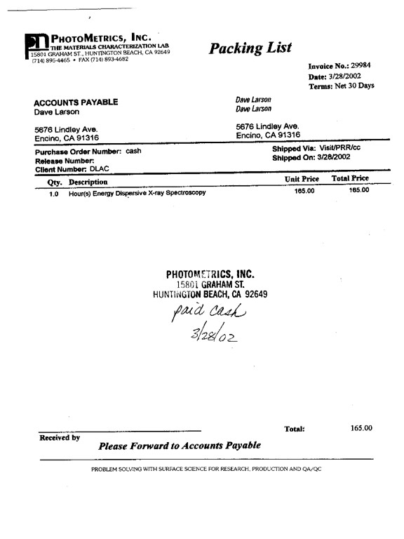
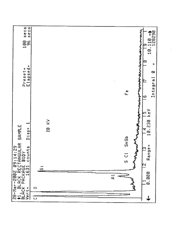
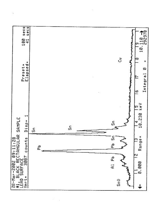
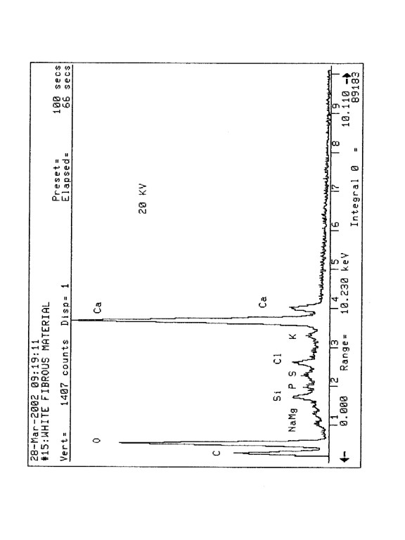
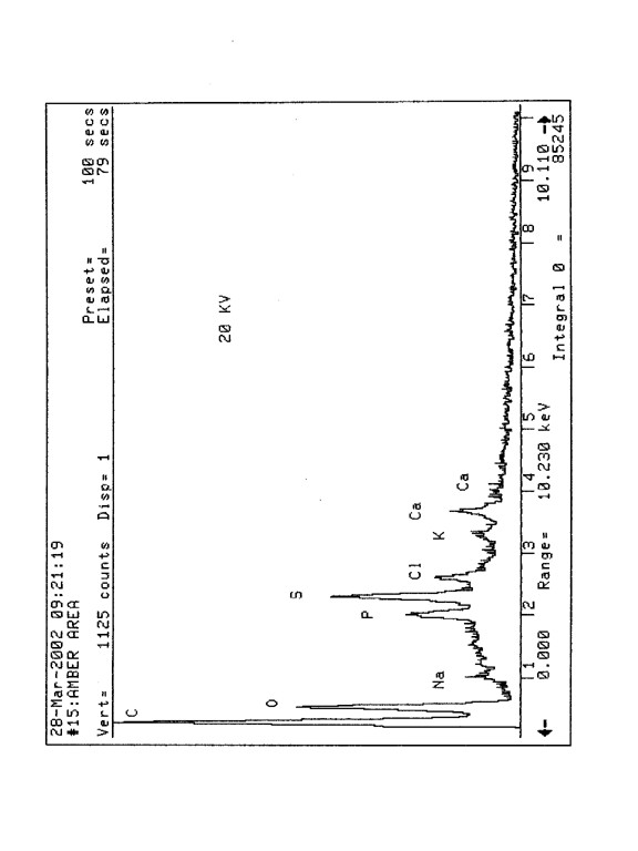
Microstimulators and Microtransducers for Functional Neuromuscular Stimulation
Principal Investigator Affiliation Contract Number Link
Joe Schulman, Ph.D. A.E. Mann Foundation N01-NS5-2325
ARTICLE C.1 BACKGROUND
The Neural Prosthesis Program (NPP) of The National Institute of Neurological Disorders and Stroke is
committed to the development of safe, reliable, and effective systems for functional neuromuscular
stimulation (FNS) in spinal cord injured individuals. Multiple implantable microstimulators which selectively
stimulate paralyzed muscles in a controlled fashion may permit an individual to use his or her own muscles
as the motors to produce limb movement. Multiple implantable microtransducers that sense contact, grasp
force, and limb position from either implanted transducers or intact sensory receptors may provide sensory
feedback from an otherwise insensate limb. To produce a useful system, these sensory and motor
prostheses are being developed together as standard and compatible building blocks of an integrated FNS
system.
The NPP is supporting research and development of a system consisting of an extracorporeal coil and a
family of implantable microstimulators and microtransducers (Loeb et. al., Injectable microstimulator for
functional electrical stimulation., Med. & Biol. Eng. & Comput. 29:NS13-NS19, 1991; Troyk and Schwan,
Closed-loop class E transcutaneous power and data link for microimplants., IEEE Trans. on BME 39:589-
599, 1992). The system is designed to power and control up to 64 individual transducers and stimulators
through a single external coil. During the past five years significant progress has been made in developing
addressable, implantable microstimulators and an extracorporeal coil and transmission system. This work
has progressed to the point where first generation devices are available for implantation. Work was also
begun during the past 2 years on the development of implantable addressable transducers. This contract will
continue the engineering development of the microstimulators and transducers. In addition, in-vivo evaluation
of these devices will be initiated in an animal model.
This RFP represents a competitive renewal of an ongoing contract. Copies of progress reports from current
contracts related to this work and a bibliography of Neural Prosthesis Program publications are available
from the Contracts Management Branch, Room 901 Federal Bldg., 7550 Wisconsin Ave., Bethesda, MD
20892.
ARTICLE C.2. STATEMENT OF WORK
Independently, and not as an agent of the Government, the Contractor shall exert its best efforts to develop
and test a system for functional neuromuscular stimulation (FNS) consisting of implantable receiver-stimulators
and transducer-telemeters and an easily donned extracorporeal transmitter.
Specifically, the Contractor shall:
A. Design, fabricate, and test implantable receiver-stimulators, implantable transducer-telemeters, and an
extracorporeal transmitter for FNS.
1. The implantable receiver-stimulators, consisting of power receiver, control receiver, stimulus and control
circuitry, electrodes, and encapsulation shall meet the following specifications:
a. They shall be made as small as possible while still being compatible with the other requirements described
below. The target volume of each stimulator shall be 60 cubic mm or less.
b. An individual stimulator shall initiate a stimulus pulse only in response to a properly addressed command
from the transmitter. There shall be at least 64 different stimulator addresses that can be selected.
c. The stimulators shall derive their power and commands by an inductive link from a transmitter coil with
field specifications as outlined below.
d. The stimulus current waveform shall have two phases of opposite polarity. The duration of the first phase
shall be variable from 0 to 200 microseconds in at least 200 steps on a pulse by pulse basis.
e. The stimulus current level of the first phase of a stimulus pulse shall be adjustable and shall include levels
of 1 and 10 milliamps under control of the transmitter. The current of the second phase shall guarantee long.34
term charge balance at the electrodes under all pulsing conditions within specifications. Stimulator
compliance voltage shall be at least 10 volts.
f. Stimulating electrodes shall be made of corrosion resistant and biocompatible materials (e.g. platinum,
platinum-iridium, iridium, or tantalum pentoxide) and shall be stable in physiologic saline at 37 degrees C for
at least 1 year at the maximum charge delivery rate.
g. The stimulator shall be encapsulated in a manner that permits stable operation in physiologic saline at 37
degrees C for at least 1 year with materials that are known to be biocompatible.
2. The implantable transducer-telemeters consisting of transduction unit, power receiver, control circuitry,
digitizer, telemetry circuitry, and encapsulation shall meet the following specifications:
a. The transducer-telemeters shall not interfere with the operation of the receiver-stimulators and vice-versa.
b. The transducer-telemeter package shall occupy a volume of no more than 125 cubic mm (not including
magnets, electrodes, or other passive elements which can be external to the package if they are needed for
the design). Biocompatibility and life expectancy shall be as specified for the microstimulator in part 1.
c. The transducer-telemeters shall derive power and commands from the same transmitter coil as the
microstimulators and shall transmit information to this coil upon command.
d. The transducer-telemeters shall be addressable with at least 64 unique addresses using an addressing
scheme that is compatible with the microstimulator addressing.
e. The telemeter's digitizing and telemetry circuits shall be designed to provide at least 8 bits of digital data
per sample. Signal conditioning for sensing biopotentials suitable for closed-loop control and/or sensory
feedback shall be incorporated in telemeters with addresses 1 through 16.
f. A joint angle transducer-telemeter shall be designed to provide wrist joint angle information for use as a
command signal with a resolution of at least 5 degree as the wrist moves through its physiological range of
flexion and extension. The error of angle measurement (including drift, hysteresis, and errors due to wrist
movement other than pure flexion and extension) shall not exceed 15 degrees.
3. The extracorporeal transmitter shall meet the following specifications:
a. The transmitter field shall permit specified operation of the stimulators and transducers anywhere within a
cylindrical shaped volume of physiologic saline at least 9 cm. in diameter and at least 16.0 cm in length.
b. The transmitter field shall permit specified operation with up to 10 degrees of axial misalignment between
the transmitter coil and the receiver coils in the stimulators and transducers.
c. The transmitter, under the control of a computer, shall be capable of powering and controlling at least 64
stimulators and/or transducers in any combination.
d. The transmitter coil shall be designed to be donned and doffed as easily as an item of clothing.
e. The transmitter shall operate reliably in the presence of electromagnetic interference commonly found in a
home or work environment.
4. The Contractor shall make its best effort to deliver to the Project Officer one set of 32 receiver-stimulators
each with a different address, one set of 4 joint angle transducer-telemeters each with a different address,
and one transmitter with specifications as outlined above by the end of the contract period.
B. Select a suitable animal model and evaluate implanted microstimulators in this animal model.
1. Evaluate the tissue reaction to implanted stimulators placed intramuscularly and subdermally for periods of
at least 3 months.
a. Evaluate the tissue reaction to active and inactive devices.
b. Evaluate the tissue reaction to any components used in making the device that might be exposed to tissue
should the encapsulation fail.
2. Investigate the threshold stability and motor recruitment stability of microstimulators over a period of at
least 3 months.
3. Investigate the function of implanted transducer-telemeters over a period of at least 3 months.
C. Cooperate with other investigators in the Neural Prosthesis Program to integrate this work into practical
FNS systems..
Multichannel Transcutaneous Cortical Stimulation System
Principal Investigator Affiliation Contract Number Link
Phil Troyk, Ph.D. Illinois Inst. of Technology N01-NS7-2365
BACKGROUND
The Neural Prosthesis Program (NPP), National Institute of Neurological Disorders and Stroke, National
Institutes of Health develops implanted devices that interface directly with the nervous system to replace or
supplement function in neurologically disabled individuals.
Significant advances have been made in demonstrating the feasibility of bypassing peripheral sensory
organs such as the ear and the eye to restore lost sensory functions. Recently, a blind individual had an
array of 38 microelectrodes with percutaneous leads implanted into her visual cortex for a period of three
months. During this time she was able to see and describe visual phosphenes produced by electrical
stimulation through the microelectrodes. Critical engineering parameters, such as phosphene thresholds as
low as 4 microamperes and a two point resolution of 500 microns, were determined which now permit the
design of a permanent implant controlled by electromagnetic signals passing across the skin. (Ref.
Hambrecht, F.T., 1995, Visual prostheses based on direct interfaces with the visual system. In Brindley, G.S.
and Rushton, D.N. eds., Baillière's Clinical Neurology: Neuroprostheses, Baillière Tindall, London, pp 147-
165.) Because such a permanent implant would not require any leads passing through the skin, there should
be little risk of infection and the implant could be left in place indefinitely.
Specifically, a transcutaneous stimulation system consisting of a computer controlled transmitter and a group
of implantable receiver-stimulator modules, each with 256 stimulus channel outputs, is needed. Research
and development are required to assure that the implanted portion of this system will be small enough to fit
safely and comfortably beneath the scalp and that the stimulus outputs are flexible enough to provide the
range of stimulus parameters necessary for producing patterns of phosphenes by intracortical
microstimulation. This transcutaneous transmission system will interface not only with discrete wire
microelectrodes but also with silicon microstimulating microelectrodes presently being developed by other
investigators in the NPP. The extracorporeal portion of the system will include a computer controlled
transmitter for sending power and control signals across the skin to the implanted receiver-stimulator
modules.
This contract research is a new project not previously supported by the NPP. A bibliography listing
publications resulting from NPP studies related to this project is available, free of charge, from the Neural
Prosthesis Program, NIH, Federal Building, Room 916, Bethesda, MD 20892-9170. (fax: 301-402-1501, e-mail:
fh2@cu.nih.gov)
STATEMENT OF WORK
I. Independently, and not as an agent of the government, the contractor shall exert its best efforts to design
and fabricate a transcutaneous transmission system suitable for use in a human visual prosthesis. The
system shall consist of: 1.) a group of appropriately packaged, implantable, 256 channel receiver-stimulator
modules each with high density connectors suitable for connection to 256 cortical microelectrodes; 2.) an
external transmitter interfaced to an external computer which can be used to control the implanted receiver-stimulator
modules; 3.) a reverse telemetry system for monitoring key voltages in the receiver-stimulator
modules. The contractor will not be required to furnish the microelectrodes nor perform any animal or human
testing.
Specifically the Contractor shall:
A. Design the overall system such that it can be expanded in modules of 256 channels up to 1024 channels.
B. Design the receiver-stimulator module to meet the following target specifications. (Note: Priorities and.36
limits will have to be assigned to some of the stimulus parameters under certain operational conditions to
avoid conflicts. These rules of operation will be established shortly after the beginning of the contract in a
joint meeting between the contractor and the Project Officer.)
1. Capable of passing truly simultaneous biphasic current pulses through at least 16 of any of the 256
microelectrodes that will be connected to its output with the capability of passing interleaved biphasic current
pulses through any or all of the non-simultaneously pulsed microelectrodes.
2. Capable of stimulating each channel at repetition rates of 10 to 250 Hz. The repetition period should have
a resolution of 250 microseconds.
3. Phase durations of each phase of a biphasic pulse pair controllable over the range of 50 to 750
microseconds (50 microsecond resolution/phase)
4. Output compliance voltages of at least +/- 5 volts.
5. Amplitude of each phase controllable over the range of0 to +/- 64 microamperes (0.5 microampere
resolution) unless limited by the compliance voltage.
6. Have an anodic bias supply adjustable over the range of 0 to 0.75 volts referenced to a standard calomel
electrode (SCE). In a functional system, the actual voltage of this bias must be translated to correspond to
the use of a large surface area platinum reference electrode that will be used in place of a SCE. Each
channel must be connected to the anodic bias supply through large bias resistors (e.g. 10 megohm)
7. Train length on each channel of 1 to 255 biphasic pulse pairs.
8. Train delay times for each channel referenced to a reference timing pulse (e.g, a reference pulse for
channel #1) adjustable over the range of 0 to 12700 microseconds (100 microsecond resolution).
9. Maximum total output current of each module at least 1024 microamperes.
10. Have built-in safety features that include the ability to sense the failure of any of the output drivers or
other modes of operation that could result in charge imbalance and tissue damage.
a. Since it is assumed that space will not permit output coupling capacitors on each channel, a desired
feature would be the ability to disconnect a shorted output driver from its power supply.
11. The modules should be capable of independent operation, i.e. should any of the modules fail, such
failure should not affect the operation of the remaining modules.
12. Have a reverse telemetry system for monitoring the following voltages within each module on demand
a. The voltage waveform developed across any remotely selected microelectrode during stimulation.
b. The anodic bias supply.
c. The positive and negative power supply voltages
13. Contained in a hermetic package
a. Suitable for implantation between the scalp and the skull with dimensions no greater than 5 mm thick, 30
mm wide, and 30 mm long, not including any receiving antennae which can be external to the package.
b. With 4 separate 66 contact, high-density, low disconnect force, connectors in the package walls that
interface with appropriate connectors terminating the leads from the microelectrodes or on dummy loads
during in-vitro testing..37
c. With smooth, rounded edges and attachment sites for immobilizing the package to the skull in an
appropriate manner.
C. Design the external transmitter portion of the system to supply power and full control of up to four
receiver-stimulator modules.
1. The transcutaneous transmission signal should be capable of reliably operating through human scalp
tissue with thicknesses ranging from 2 mm to 10 mm.
2. The transmitter shall be under the control of a computer whose output can be altered by keyboard entries,
by software or by a remote interface that will eventually be controlled by an image sensing device such as a
television camera. (The contractor does not need to supply the image sensor, nor any interface electronics
between the image sensor and the computer, only the remote interface that will allow full control of the
receiver-stimulator modules.)
3. Although the external portions of the systems to be supplied under this contract do not need to be "patient
portable", the design should not ignore the fact that future generations of the system will be portable.
D. Fabricate and test, in-vitro, a complete system with 1024 channels.
1. Document the ability of the system to deliver the specified design stimuli at the specified rates without
significant cross talk between channels.
2. Test functional receiver-stimulator packages with integral connectors for hermeticity and proper electrical
operation in an accelerated aging environment of heated saline solution for a period of at least 6 months.
E. Before the end of the first year of the contract, furnish the Project Officer with 5 empty but hermetically
sealed receiver-module packages with at least one 66 contact connector for in-vivo testing by other
investigators in the Neural Prosthesis Program (NPP).
F. Before the end of the second year of the contract, furnish the Project Officer with at least 5 fully functional,
256 channel systems, complete with mating connectors so that other investigators in the NPP can attach
microelectrode leads and test the complete system in animals.
G. Before the end of the third year of the contract, furnish the Project Officer with at least 2 fully functional,
1024 channel systems, complete with mating connectors for attachment to microelectrode leads for human
testing by other NPP investigators.
H. Should failures occur during the above mentioned in-vitro or in-vivo testing, the remaining required
deliverables will be reduced, upon mutual agreement between the contractor, the Project Officer and the
Contracting Officer, to allow resources to be applied to the redesign and fabrication of relevant parts of the
system.
I. The contractor shall coordinate his work, through the Project Officer, with other investigators in the NPP..
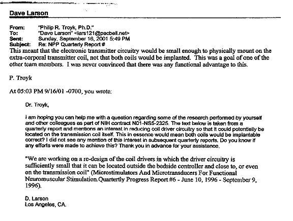
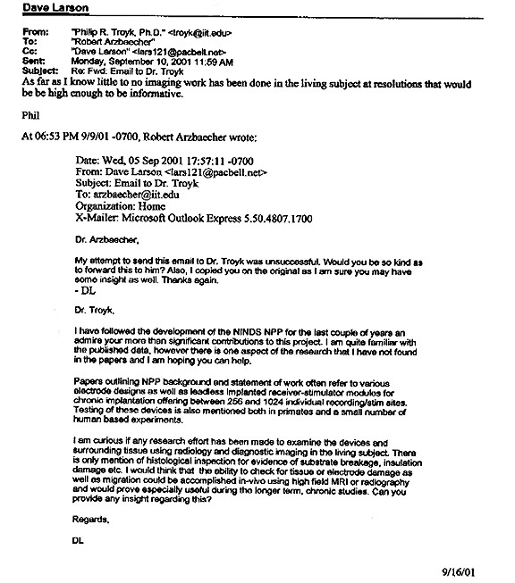
-----Original Message-----
From: Dave Larson [mailto:lars121@pacbell.net]
Sent: Friday, January 25, 2002 10:42 PM
To: hajimiri@caltech.edu
Subject: CMOS ASIC Question......
Ali,
Hello and happy new year. You probably don't remember me as I have only met you once on campus. I
occasionally depend on the help of Steve Potter and others in Biomedical Imaging Center for help with
Physiology studies etc., however I find myself in need of help regarding Integrated Circuits and Sensors.
1. If developing ASIC for implantable microstimulator for functional nerve stimulation (FES), mention is made
in various papers of both CMOS and Bi-CMOS process. Can you provide a general or "approximate" idea as
to what kind of yields from wafer are typically achieved in this process? Assume 3.0µ or 1.2µ process
through MOSIS run?
The yield is usually very high (better than 99%) on those processes.
2. When testing chips and assemblies, what factors are used in determining the amount of difference in
carrier levels? I have seen reference made to the lower level at 80% or 90% of the upper level. I am trying to
determine what factors would require a greater depth of modulation to be desired.
Consider the following: If one were to multiplex a single electrode driver to multiple electrode sites and
assuming a nominal stimulation rate of approximately 30 Hz, 10 to 100 electrodes could share a common
driver provided that temporal and phase modulation of individual electrodes were not required for control. In
such a scheme, creative circuit techniques would be needed to insure electrode charge recovery. Could this
configuration require a greater depth of modulation?
I quite frankly don't follow this question entirely. If the question is how many electrodes can you control using
one wireless driver, the answer is quite a few, if you use the right coding schemes. In general this depends
on a large number of factors, such as bandwidth, the sophistication of the electrode function and the
frequency of stimuli.
In an ASIC design that functioned appropriately at 5 volt compliance, and then encountered latch-up
problems when redesigned for 20 volt compliance, how difficult do you think this problem would be to
correct? If the process plays a significant role, consider the problem for both 3.0 and 1.2µ CMOS through
MOSIS run.
Latch up is primarily determines by the substrate doping level, and is usually avoided by following the design
rules, including, but not limited, to close proximity of substrate contacts with the active devices. In general it
is not advisable (at all) to use a process qualified for 3 or 5 volts with higher voltages. Even if the circuits
work, you will have reliability and longevity problems.
Many thanks for your assistance and best wishes.
Dave Larson.41
Mr. Larsen: In going through my efiles as part of my year-end cleanup, I did not have a clear record that the
following response was actually sent to you with regard to your September inquiry. Hence, I am sending it
to you now. My apologies if it duplicates an earlier transmittal.
Donna J. Dean, Ph.D.
Acting Director
National Institute of Biomedical Imaging and Bioengineering
Building 31, 1B37, MSC 2077
National Institutes of Health
Bethesda, MD 20892-2077
Phone 301-451-6768
Fax 301-480-4515
deand@nibib.nih.gov
http://www.nibib.nih.gov
Dear Mr. Larson,
I have asked some people at NIH for an informed opinion on your query and am pleased to transmit the
following response.
There are several parts to this inquiry, but basically the concern is the possibility that a clinical researcher
could could implant a clinically undetectable (with standard imaging methods) probe without approval to do
so. A second part is if NIH is considering this possibility.
With regard to unapproved implantation, there is always the chance that a researcher could perform such an
implant in conjunction with other clinical research activities without approval or without including this in the
reviewed research protocols. Patient rights and informed consent are major concerns for clinical research,
and the NIH requires stringent reviews of clinical procedures and on-site monitoring of clinical research for
their funded grants. However, a knowledgeable researcher absolutely intent on implanting a sub-millimeter
size probe may be able to find a way to do it during experimental activities.
Information obtained in such a manner could not likely be published in a reputable journal, since the
methodology would have to be part of the article, which makes it less tempting if the unethical clinician is
seeking acclaim. Also, the fact that such work could not then be replicated by others would heighten the
likelihood of scrutiny and ultimately, exposure as fraud.
Is possible unethical research of concern to the NIH? Certainly. There is a Bioethics Office that explicitly
deals with such issues, and the Office of Extramural Research coordinates clinical research requirements for
NIH grantees for all the NIH research institutes and centers. On-site reviews of NIH-funded clinical research
are conducted by NIH staff to evaluate compliance with patient rights issues and adherence to planned
experimental protocols. The issue of unauthorized implants is one of many causes for concern in the
general realm of unethical clinical research, and the NIH endeavors to deal with such issues before and
during clinical investigations.
By way of information, all micro devices that are capable of sending signals into or out of the body are readily
detectable using relatively standard x-ray imaging methods. You are correct that we use extensive
histological analysis to evaluate the tissue response to implanted micro devices. This is not because we
cannot detect the devices using x-rays but because there is a need to do safety studies that involve detailed
light and electron microscopic analysis of the tissue response at a cellular and subcellular level.
The question of informed consent applies to all research involving human volunteers and is clearly one of
increasing importance in light of recent shortcomings. Informed consent as outlined in the Belmont Report
and subsequent guidelines as well as trust between the physician and human volunteers is essential for
ethical research and should be a high priority at NIBIB as well as at the other institutes..42
-----Original Message-----
From: Dave Larson [mailto:lars121@pacbell.net]
Sent: Tuesday, September 18, 2001 4:10 PM
To: Dean, Donna (OD)
Cc: Leonard, Laurie (NINDS); Wheeles, Timothy (OD)
Subject: NIBIB Information
I have a question and I am hoping you can provide some insight. Current research in the NIH/NINDS Neural
Prosthesis Project (NPP) has led to the development of implantable sensors and probes (Professors Troyk,
Najafi, Banks etc., PI on NIH NPP contracts) that are just below the size of feature detection in typical clinical
radiology (MRI/CT etc). Continuing research on animal models and a select few human cases show that
these probes can not be imaged and the only means of examination is a histological method after the
research subject dies with no in-vivo examination due to the sub-millimeter size. The MRI capability of a
clinical MRI system (1.5T) is in no way capable of imaging an object below 500x500 microns, however there
is development of new high field MRI as high as 7.0T and research at Caltech has used fields as high as
11.7T in rodents. My question Donna pertains to the potential that exists for an unethical researcher to
implant probes in an unwilling human in order to gain long-term research data that is otherwise unattainable
in animal models. The work of Professors Loeb and Troyk also involve passive, radio frequency teqniques
that make remote sensing and stimulation of the probes attainable. If this were to happen, there would be no
way to detect the probes in a clinical situation and begin any treatment for the potential victim/subject. A
horrible thought, yes, but it appears to be a potential cause for concern at this moment. Do you think the
establishment of the NIBIB will address this, or has anyone in the NIH addressed this issue at all? Many
thanks for your help.
David A. Larson
Los Angeles, CA
Dr. Kerns received a Ph.D. in Electrical Engineering from the California Institute of Technology and has been kind
enough to take an interest in my situation and I am grateful because his knowledge of implantable devices and
experience with integrated circuits and sensors has been very beneficial. His prior professional experience includes:
Senior Analog Designer, Analog Devices, Inc. (A leading manufacturer of high performance analog and digital IC's)
Staff Scientist, Tanner Research (IC design, simulation and layout software development), and Dr. Kerns has also
worked for the Jet Propulsion Laboratory and Fermilab.
Date: Tue, 19 Feb 2002 12:16:27 -0500 (EST)
From: Kernsd@---------
Subject: Re: Hello?
Dave,
Your "wirebond" pic does look very much like a
single wirebondfrom a substrate to the top of a die,
but I would have expected at least two bonds to
a device capable of wireless communication and
local stimulation. My opinion is certainly not the last word.
It looks like you're making good progress in
pushing forward the analysis of the object.
- Doug K
"flip-chip" is an assembly process for connecting.43
an IC chip to other electronic devices. The process
essentially consists of soldering the chip face-down
(hence the name "flip-chip") onto the other stuff.
Flip-chip assembly is full of technical hassles, but
it's one of the most compact assembly techniques
yet invented. The truly most-compact I've ever seen
is "chip stacking." That has hassles that make
flip-chip seem like a walk in the park, but there are
still people who care so much for compact stuff
that they'll pay the outrageous prices.
I hope that's helpful.
- Doug K
----- Original Message -----
> From: <Kernsdou----------
> Sent: Sunday, January 20, 2002 1:47 PM
> Subject: Re: semiconductor technical stuff....
Chip stacking is the assembly technique of gluing
several silicon chips together, typically adding
metal interconnections between the layers of the
stack by lapping the edges and doing the usual
evap/resist/litho/etch process that's used to make the
chips in the first place. The hassles one encounters
are usually of two types:
(a) one of the chips in the stack is flawed, so it
doesn't work correctly, and it's difficult to discover
the flaws prior to assembling the stack. The end result
is that the stack containing the flawed chip has to be
thrown away, even though most of it is composed of
good pieces. Sometimes a flaw can be caused by the
stacking process, so even if you start with chips that
are all known to be good, the stack may still be
flawed after assembly.
(b) The interconection between chips in a stack may have
flaws, so there's a missing connection or a shorted
connection. Again, the stack may have to be thrown
away, even if all the chips were good..44
> I believe that the implanted devices have on-chip
> > memory allowing "event-related" or closed-loop stimulation. This would
allow the
> > use ofnaturally occurring eventsto triggera stimulus response
> > from the implant. I have noticedthat when I'm on vacation or in the
> > faraday cage that the stimulus isconsistent in it's properties andis
> > event related which is in contrast to the stimulus that I am typically
forced to
> > endure which is more spontaneous and random in it's occurrence as well
as it's amplitude and duration.This leads me to believe that even if I am able
to disrupt the signal, I will still be subject to
> > closed-loop, event related stimulus. I believe this is made possible by
an electrode made from tantalum which is able to act as a capacitor which
stores a
> > charge derived from an electrolytic/voltametry condition resulting from
> > interaction with the body fluid, or perhaps the implantable devices
> > cancontinue tostore a charge from a carried signal even if the data
> > comm is non-functional. I'm trying to assess what wireless communication
method
> > would be feasible for commandof the implants andwhat possible
> > counter-measures may exist. I'll assume
> > that the individual responsible for this is licensed by the FCC and has
his own
> > little piece of the spectrum unless a programmable micro-controller
would allow
> > variety of frequencies to be used.I'm wondering if a frequency in the
> > vicinity of 220.000 MHz as the carrier signal and amateur radio relay
used to
> > establish a network is being used. If this were the case, what equipment
would I
> > need to purchase that would be capable of jamming this signal and what
kind of trouble can I create by attempting to disrupt the signal? Can a specific
> > frequency be targeted in a manner that would not cause problems
elsewhere, or is
> > the idea to simply stomp on everything in the vicinity with noise and
power?
> > Thanks for your insight Doug.
> >
> > Sincerely,
> >
> > Dave Larson
Hi David,
EDS would NOT be able to identify an epoxy polymer.
FTIR would be ble to identify it as an epoxy, but probably not a specific type. However, if it is not epoxy and
is some other polymer FTIR would be able to determine that.
With EDS, epoxies, urethanes, acrylics.... all look like they are carbon and oxygen.
If you are interested in the FTIR let me know, I will have Greg ansten call you.
If you would like to schedule an appointment for EDS let me know
Thanks
Paul Reidel
PhotoMetrics
(714) 895-4465.45
<lars121@pacbell.net>; Mon, 10 Dec 2001 14:41:21 -0500 (EST)
Date: Mon, 10 Dec 2001 14:42:45 -0500
From: Stuart Cogan <scogan@eiclabs.com>
Subject: Re: Implantable Microstimulators
Dave,
We have only a little experience evaluating tissue.
If the tissue samples are in an appropriate form we can look at them with the electron microscope and
probably identify the chemical nature of the substances that may be foreign bodies. This we have done with
specially prepared histology slides with some success.
If you want to discuss this further, please feel free to call me.
Regards
Stuart Cogan
EIC Laboratories, Inc.
1 781 769-9450
<lars121@pacbell.net>; Fri, 01 Feb 2002 17:52:42 -0500
Date: Fri, 01 Feb 2002 17:56:00 -0500
From: wise@umich.edu
Subject: Re: Supply Voltage
The level shifter problem was just a design error. The output bus
has a fair amount of capacitance and the driver was too small to
drive it quickly. The best solution was to resize the driver, which
we have done. But with the existing probes, another solution that
helped a bit was to increase the voltage. This isn't desirable long
term because it puts more stress across the encapsulating
dielectrics. We would like the probes to operate as low in voltage
as possible to minimize our packaging problems; however, ultimately,
we are limited by the water window and the spreading resistance drops
in the solution. They make it hard to operate below 5V for small
sites. So the voltage is really a trade off between device site size
and the needed stimulating current levels. Hope this helps a little.
... Ken D. Wise, Professor.
>Professor Wise:
>
>Hello, and greetings from California. I have recently had the
>opportunity to read published papers regarding micromachined stim
>electrode arrays and one your papers mentions level shifters that
>operate slower than which is desired. You acknowledge that an
>adjusted (higher I assume) voltage is a solution, but only for
>present day use. Why would adjusted voltage not be a solution for a
>"standardized" device? Thank you for your insight and any help you
>may be able to provide.
>
>Regards,
>
>Dave L
>Northridge CA.46
> There is a new 8.0T system at OSU which can image particle sizes of
> 200umx200umx2000um, so new advances in imaging are becoming attainable
Petra Schmalbrock Ph.D.
Associate Professor
The Ohio State University, Dept. Radiology
170 Means Hall, 1654 Upham Dr, Columbus OH 43210
Phone 614-293-4139
FAX 614-293-8129
![]()
Last Update: 08/06/2023 03:35 +0300

Please help keep us going and make a donation Thanks to all supporters! PayPal, Сбербанк Sberbank Visa 4276 3800 4476 1661 Copyright JAR2 2003-2103 All Rights Reserved Publishing Banned Truth Since June 06, 2003
|